SEMICONDUCTOR PROCESSING & PRODUCTION WHITE PAPERS & CASE STUDIES
phantom
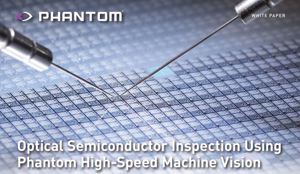
Optical Semiconductor Inspection
Optical semiconductor inspection presents complex challenges, including the diminutive size of the target and proximity of individual dies in the wafer space. This paper addresses the challenges that can arise during the semiconductor inspection process, including reticle inspection in patterned and unpatterned wafers, the identification and flagging of deformed wires, and the presence and absence of features.  Continue Reading..
FLIR T500-Series Macro Mode: Single-Lens Solution For Imaging Small Targets
Electronics inspection is one of the most common applications for thermal imaging, which typically involves finding hot spots on printed circuit board assemblies (PCBAs) and ensuring that various components are working within their design limits.  Continue Reading..
Short-Wave Infrared Cameras In Semiconductor Inspection Applications
This white paper discusses several applications of SWIR (short-wave infrared) cameras within semiconductor inspection applications, especially those that rely on the capability of SWIR cameras to see through semiconductor materials, such as silicon.  Continue Reading..
White Paper: Improving Performance In Computer To Plate Printing Using Semiconductor Laser Arrays
Over the last 25 years, electronic typesetting and desktop publishing (DTP) have revolutionized the printing industry. Almost anyone with a computer and the right software can create and print professional materials. However to achieve the highest print quality, it is still necessary to use a commercial or industrial printer with advanced technology for delivering state of the art print quality standards. By Professor John H. Marsh, Ph.D.,...  Continue Reading..
Improving Performance In Computer To Plate Printing Using Semiconductor Laser Arrays
Over the last 25 years, electronic typesetting and desktop publishing (DTP) have revolutionized the printing industry. Almost anyone with a computer and the right software can create and print professional materials. However to achieve the highest print quality, it is still necessary to use a commercial or industrial printer with advanced technology for delivering state of the art print quality standards. By Professor John H. Marsh, Ph.D.,...  Continue Reading..
Application Note: Short Pulse UV Lasers In Semiconductor Applications
Excimer and UV diode-pumped solid-state (DPSS) lasers can be used by the semiconductor industry, and others, in applications that cannot be performed by mechanical, chemical, or other laser fabrication methods. By JP Sercel Associates  Continue Reading..
Short Pulse UV Lasers In Semiconductor Applications
Excimer and UV diode-pumped solid-state (DPSS) lasers can be used by the semiconductor industry, and others, in applications that cannot be performed by mechanical, chemical, or other laser fabrication methods. By JP Sercel Associates  Continue Reading..

SEMICONDUCTOR PROCESSING & PRODUCTION PRODUCTS

The Zygo Optical Systems Division’s Tier 1 optical fabrication facility utilizes their own proprietary manufacturing and metrology techniques to design and manufacture optical components and optical assemblies for use in semiconductor applications.

SEMICONDUCTOR PROCESSING & PRODUCTION NEWS

  • Metrology is the science behind precise measurement, and its role in semiconductor manufacturing is increasingly vital as chips get smaller and more complex, powering our digital world.

  • Optical computing could be the next big thing in semiconductor production. Light has already become a go-to choice for transmitting data, but most systems still must translate photons into electrical signals to process information. All-optical chips could change that.

  • Photonic gap materials, or photonic crystals, are structures with a periodic dielectric profile that prevent light from propagating at certain wavelengths. This creates a "gap" where light cannot travel, offering potential for optical devices like filters and waveguides.

  • It’s almost show time with both Automate 2025 and the CLEO Conference just around the corner. Let’s take a look at two of the photonics industry’s most-anticipated shows.

  • From high-sensitivity detectors and adaptive optics to integrated spectrographs and space-qualified devices – photonic technologies are transforming our view of the Milky Way and beyond.

  • SPIE Photonics West 2025, scheduled for January 25–30 in San Francisco, offers numerous benefits for professionals in the optics and photonics industry. Here are 25 reasons to attend.

  • It’s that time again. Let’s take a look at the most-read articles that appeared on Photonics Online this past year. Why, it’s become an annual event!