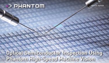
Optical Semiconductor Inspection
Source: Vision Research, Inc.

Optical semiconductor inspection presents complex challenges, including the diminutive size of the target and proximity of individual dies in the wafer space. This paper addresses the challenges that can arise during the semiconductor inspection process, including reticle inspection in patterned and unpatterned wafers, the identification and flagging of deformed wires, and the presence and absence of features. Download the full white paper to learn more.
access the White Paper!
Log In
Get unlimited access to:
Trend and Thought Leadership Articles

Case Studies & White Papers

Extensive Product Database

Members-Only Premium Content

Welcome Back! Please Log In to Continue.
X
Enter your credentials below to log in. Not yet a member of Photonics Online? Subscribe today.
Subscribe to Photonics Online
X
Subscribe to Photonics Online
