
From Silicon To System: A Custom Backscatter Electron Detector Built For Integration
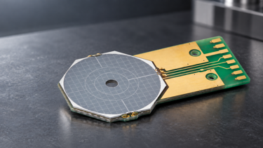
Opto Diode’s custom backscatter electron detector combines segmented silicon sensing, specialized geometry, PCB integration, and electronics to meet demanding system-level detection requirements.
From Silicon to System: A Custom Backscatter Electron Detector Built for Integration
In advanced electron detection systems, the detector itself is only one part of the measurement chain. Detector geometry, active area placement, capacitance, carrier collection, signal routing, amplification, packaging, and mechanical integration can all influence the performance of the final instrument.
This is particularly important in applications such as scanning electron microscopy and other charged particle systems, where a detector may need to operate close to the primary electron beam while collecting fast and sometimes relatively small signals from electrons returning from the sample.
Opto Diode developed its Backscatter Electron Detector as an example of how these requirements can be addressed through a combination of custom silicon detector design, wafer fabrication, packaging, PCB integration, and electronic subsystem development.
Rather than treating the detector as an isolated silicon component, the design considers how the device will ultimately function as part of a complete measurement system.
Five Independent Active Detection Areas
At the center of the design is a silicon detector incorporating five independent active regions.
Four of the active areas are arranged in a quadrant configuration around the center of the device. An additional circular active region is positioned closer to the beam axis and surrounds the central aperture.
This segmented architecture provides significantly more flexibility than a single large area detector.
Signals from the four quadrant regions can be measured independently, allowing the system to distinguish differences in electron and back scatter particle collection across different areas of the detector. Depending on the measurement technique and downstream processing, these signals can be compared, combined, or analyzed individually.
The additional circular sensing region provides another independent detection area close to the primary beam axis. This gives the instrument designer access to an additional signal channel and provides another way to characterize the spatial distribution of returning electrons and particles.
The five channel configuration therefore allows the detector to provide more than a single measurement of total electron flux. It creates the opportunity to extract spatial information from the returning electron signal and gives the system designer greater flexibility in how that information is processed.
A Central Aperture Designed Around the Electron Beam
A central aperture passes completely through the detector assembly.
This opening allows the primary electron beam to travel through the detector and continue toward the sample. Electrons that are subsequently backscattered from the sample can travel back toward the detector and be collected by the surrounding active regions.
This geometry allows the detector to be positioned directly around the beam path without blocking the incident beam.
For systems such as scanning electron microscopes, the relationship between the beam, sample, detector geometry, and working distance can have a major impact on collection efficiency and the information contained in the detected signal.
The aperture therefore becomes an important part of the detector design rather than simply a mechanical feature.
Different applications may require different aperture dimensions, detector diameters, active area arrangements, or overall geometries. These parameters can be evaluated as part of a custom detector design so that the sensing element fits the architecture of the instrument rather than forcing the instrument to accommodate a standard detector.
Electrode Geometry for Faster Signal Collection
One of the more distinctive features of the detector is the aluminum electrode pattern extending across the active areas.
Large area silicon detectors can introduce electrical challenges when response speed becomes important. As detector area increases, capacitance can become a significant factor in determining the bandwidth and response of the overall detection system.
The electrode structure used on this device is intended to help address these challenges.
When the detector is operated under a sufficiently high reverse bias, the depletion region within the silicon increases while junction capacitance is reduced. Lower capacitance can improve the electrical response of the detector and reduce the load presented to the downstream readout electronics.
The aluminum lines across the active regions also provide shorter collection paths for charge generated within the detector.
When incident electrons generate electron hole pairs within the silicon, those carriers must be collected and transferred into the external circuit. Reducing the distance that carriers must travel before reaching an electrode can improve charge collection speed.
The combination of electrode geometry and reverse bias operation therefore addresses detector speed from two directions. Capacitance is reduced, while carrier collection distances are shortened.
Together, these effects can reduce detector response time and support applications where the electron signal changes rapidly or where higher bandwidth measurements are required.
Moving Beyond the Silicon Die
The detector shown here also illustrates an important part of Opto Diode's development capabilities that extends beyond semiconductor fabrication.
The custom silicon detector is integrated directly onto a purpose designed printed circuit board.
The PCB provides electrical routing for the individual detector regions while also creating a practical mechanical platform for connecting the detector to the rest of the instrument.
This type of integration becomes increasingly important as detector systems become more complex.
A bare silicon die may provide the required optical or electron detection characteristics, but the signal still needs to be electrically connected, amplified, conditioned, and transmitted to downstream electronics.
For many customers, solving those interface challenges can require as much engineering effort as selecting the detector itself.
By integrating the detector onto a custom PCB, these issues can be considered earlier in the development process.
Electrical connections can be arranged around the detector geometry. Signal paths can be shortened. Mechanical mounting features can be incorporated. Connector locations can be selected around the available space inside the customer's instrument.
Instead of developing the detector and electronics as completely separate systems, both can be considered together.
Integrating Readout Electronics
PCB integration also creates the opportunity to move the first stages of signal processing closer to the detector.
Depending on the application, Opto Diode can incorporate transimpedance amplifiers and other analog electronics directly into the detector assembly.
A transimpedance amplifier converts the detector current into a voltage signal that can be more easily processed by downstream electronics. The relationship between the detector and the amplifier is particularly important in higher bandwidth or lower signal applications.
Interconnect length, detector capacitance, amplifier input characteristics, feedback resistance, feedback capacitance, noise, gain, and bandwidth can all influence the performance of the resulting measurement system.
Placing the first amplification stage close to the detector can reduce unnecessary interconnect length and parasitic effects while giving the designer greater control over the detector and amplifier interface.
The electronics can then be expanded further depending on the application.
Possible integration can include additional gain stages, filtering, signal conditioning, bias routing, connectors, analog outputs, and interfaces to downstream conversion or control electronics.
This allows the development effort to progress from a custom sensing element toward a more complete detector subsystem.
Customization as Part of the Design Process
The Backscatter Electron Detector represents one specific configuration, but customization is a major part of Opto Diode's approach to detector development.
Many applications cannot be fully addressed by selecting a standard detector from a catalog.
The available mechanical envelope may be different. The required active area may need to change. The instrument may require a different number of channels. The center aperture may need to be larger or smaller. Electrical bandwidth, packaging, mounting, connector placement, or readout requirements may also be unique to the system.
For these applications, the detector can be modified around the customer's requirements.
Customization can include detector dimensions, active area geometry, the number and arrangement of sensing regions, aperture dimensions, electrode layouts, electrical contacts, packaging, PCB geometry, mounting features, signal routing, connector selection, and readout electronics.
The surrounding electronics can also be designed around the performance goals of the instrument.
Transimpedance amplifier selection, gain, bandwidth, filtering, detector bias, and output interfaces can all be evaluated as part of the complete detection chain.
This approach allows the detector system to be designed around the measurement problem rather than requiring the customer to design the instrument around the limitations of an existing component.
From Wafer Fabrication to Detector Subsystem
Developing an application specific detector often requires several engineering disciplines to work together.
Semiconductor processing determines the fundamental characteristics of the detector. Packaging protects and electrically connects the device. PCB layout determines how signals leave the detector. Analog electronics determine how those signals are amplified and conditioned. Mechanical integration ultimately determines how the entire assembly fits into the customer's instrument.
Opto Diode's internal silicon detector fabrication capability provides the foundation for this development process.
From there, devices can progress through packaging, die attachment, wire bonding, PCB integration, and additional electronic assembly.
Having visibility across these stages makes it possible to consider semiconductor, mechanical, and electrical requirements together during development.
The result is a capability that extends beyond supplying a silicon detector.
Customers can begin with a measurement requirement or detector concept and work toward a device that is increasingly integrated into the architecture of their system.
A Platform for Custom Detection Solutions
The Backscatter Electron Detector demonstrates how a specialized silicon sensor can be combined with custom geometry, segmented active areas, optimized electrode structures, PCB integration, and application specific electronics.
Its five independent detection regions provide spatially resolved electron measurement, while the central aperture enables integration directly around the primary beam path. Aluminum electrode structures and reverse bias operation support faster charge collection and reduced capacitance, while the custom PCB provides a practical interface between the detector and the larger instrument.
More importantly, the assembly demonstrates a broader development approach.
The detector geometry, packaging, electronics, and system interface do not need to be treated as fixed elements.
For applications requiring different active areas, channel configurations, aperture dimensions, bandwidth, packaging, or electronic interfaces, the architecture can be adapted around the needs of the measurement system.
By combining custom silicon detector fabrication with packaging, PCB development, transimpedance amplification, analog electronics, and system level integration, Opto Diode can support detector development from the wafer fab through a more complete sensing subsystem.
For engineers developing specialized scientific, semiconductor, medical, aerospace, industrial, or laboratory instrumentation, that flexibility can provide a path from an application requirement to a detector solution designed specifically for the system in which it will operate.