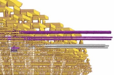
X-Rays Create 3D Images Of A Microchip's Interior
By Jof Enriquez,
Follow me on Twitter @jofenriq

Scientists at the Paul Scherrer Institute (PSI) have used a technique called X-ray ptychography to image a microchip's internal structure in three dimensions. It’s the first time a non-destructive method has clearly visualized the paths of a chip’s internal wiring (just 45 nanometres — 45 millionths of a millimetre — wide) and its 34-nanometre-high transistors without distortions or deformations.
Today, finished chips typically are checked using a method called focused ion beam/scanning electron microscope imaging (FIB/SEM), wherein layer after layer of the chip is cut and imaged with an electron microscope to check if nanoscale components are up to specifications.
Over the last several years, PSI researchers have developed a non-destructive alternative to imaging integrated circuits using lasers beamed from the Institute's Swiss Light Source. Using a technique called X-ray ptychography, the researchers directed a laser at specific spots of an Intel G3260 processor sample. A detector then measured the X-ray light pattern after it passed through the structure. The step was repeated at different angles until the chip's three-dimensional internal structure was reproduced.
"X-ray ptychography — a high-resolution coherent diffractive imaging technique — can create three-dimensional images of integrated circuits of known and unknown designs with a lateral resolution in all directions down to 14.6 nanometres," wrote the researchers in the journal Nature.
At that resolution, images are finer than any other technique can provide. But images of individual transistor components turned out fairly blurry, according to IEEE Spectrum. The resolution can be improved, though, by a factor of 1000, through improvements to X-ray sources and to other parts of the experimental apparatus, say the researchers.
Also, the Intel chip featured in the researchers’ proof-of-concept was produced using the Intel’s 22-nm process, and researchers will need to further sharpen their technique to image structures in even finer detail — such the current state-of-the-art 14-nm chips, as well as 10-nm chips in production soon.
The team also is working to extend its technique to be able to scan entire microchips, rather than just portions of chips, and to be able to image the same spot repeatedly to monitor changes when exposed to external stimuli.
"Our experiments represent a major advance in chip inspection and reverse engineering over the traditional destructive electron microscopy and ion milling techniques. Foreseeable developments in X-ray sources, optics and detectors, as well as adoption of an instrument geometry optimized for planar rather than cylindrical samples, could lead to a thousand-fold increase in efficiency, with concomitant reductions in scan times and voxel sizes," they wrote in Nature.
Jerry Hastings, a professor at the SLAC National Accelerator Laboratory in Menlo Park, Calif., agrees and told Spectrum, “I don’t see any other probe that could image a full processor without slicing it up. You need something that simultaneously gives you the resolution and the penetrating power. And that’s where X-rays are unique.”
