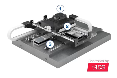
Wafer Inspection And Metrology

The manufacturing of computer chips requires a high level of precision and accuracy, as defects can cause significant setbacks. Wafer inspection and metrology play a crucial role in ensuring the quality and reliability of the final product. As chip production processes become more complex and involve hundreds of meticulous steps, it becomes increasingly challenging to maintain this level of precision. That's where PI's fast scanning and characterization solutions come in.
These solutions offer a comprehensive approach to meet the need for precision and efficiency in the chip manufacturing process. From detecting defects and edge placement errors to high-dynamic laser focus control, PI's motion solutions enable high-throughput operations, while reducing costs and increasing reliability. Let's take a closer look at the key features of these cutting-edge motion solutions designed to meet the demands of modern chip manufacturing.
Get unlimited access to:
Enter your credentials below to log in. Not yet a member of Photonics Online? Subscribe today.
