
Toward Ultra-High-Bandwidth Vertical-Cavity Surface-Emitting Lasers

A novel design and fabrication process enables high-performance, three-terminal optical transmitters
Vertical-cavity surface-emitting lasers (VCSELs) have evolved as the emitters of choice for short-distance high-speed data communications, thanks to their low cost and high power efficiency. The next generation of VCSELs is presently being optimized for modulation rates up to 25Gbit/s, but demand for bandwidth at all levels of the optical communication network is expected to reach serial data rates as high as 40–100Gbit/s in the next few years. Such requirements constitute a considerable challenge for optical transmitters and calls for radically new design concepts.
One such concept is the transistor laser, first demonstrated in 2005, which promises significantly increased modulation speed.1 This three-terminal electrical device also has an optical output. It consists of a high-frequency transistor that is homogeneously integrated into the laser. As such, it is expected to have a number of unique properties with implications for high-speed computing and optical communication, including improved modulation bandwidth, linearity, and noise properties, as well as novel functionality made possible by the additional terminal.1
Transistor-VCSELs (T-VCSELs) combine the functionality of transistor lasers with the inherent advantages of VCSELs and, thereby, provide a potential route to low cost, low power consumption, and superior performance in digital and analog applications. However, these devices are presently at an early stage of development. Their 3D structure requires greater control of voltage and current distributions, and this makes them much more difficult than edge-emitting transistor lasers to design. It also makes the contacting of the different terminals more challenging, and the short cavity is more sensitive to optical loss imposed by the highly doped base region. Even so, numerical simulations have shown that these are practical rather than fundamental problems, and that T-VCSELs do indeed have a great potential for high-frequency operation that may break the bandwidth bottleneck of conventional diode lasers.2 However, so far, T-VCSELs have only been operated at low temperatures and at modest power levels.3
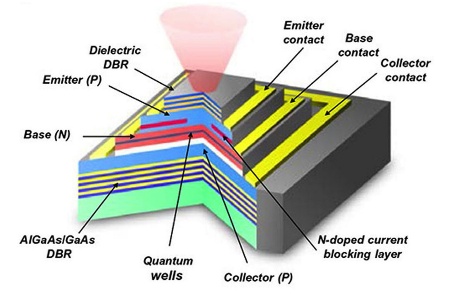
Unlike typicalcommunication VCSELs that use conducting mirrors and oxidation confinement to inject current, our design employs a novel epitaxial regrowth process that allows the cavity region to be defined by optical lithography.4It is based on a triple intracavity current-injection scheme that reduces the series resistance and allows for a low-loss optical cavity by virtue of undoped mirrors and carefully designed doping profiles. In our top-emitting and top-contacted T-VCSEL (see Figure 1), the current-blocking layer is defined by selective area epitaxy. The top and bottom mirror structures consist of silicon/silica and gallium arsenide/aluminum gallium arsenide (GaAs/AlGaAs) distributed Bragg reflectors, respectively, where a surface structuring of the former provides an option for single or multimode emission. Three compressively strained indium gallium arsenide/gallium arsenide (InGaAs/GaAs) quantum wells provide the optical gain, and an inserted high-bandgap AlGaAs layer at the bottom of the emitter forms a heterobarrier with the GaAs cavity of importance for the transistor current gain.
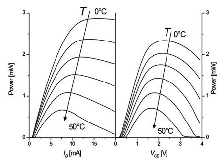
Figure 2 shows temperature-dependent light-current-voltage characteristics of a fabricated 980nm T-VCSEL with an active area of 10×10μm2. In a similar way to a conventional diode laser, the optical output power increases rapidly above a well-defined threshold current (below 1mA at room temperature) but also saturates at higher currents due to device self-heating. The maximum power decreases rapidly with increasing environmental temperature but is still around 0.5mW at 50°C: see Figure 2(left). We expect a different spectral alignment between the active layer gain maximum and the emission wavelength would improve the high-temperature performance. This is a standard optimization for VCSELs, and the reported output power and temperature-dependency compare reasonably well to standard 980nm VCSELs. The right panel of Figure 1b demonstrates the voltage-controlled operation of the T-VCSEL. Here, the collector-emitter voltage is swept while the base current is kept at a constant value. This voltage-driven mode of operation is unique to transistor lasers and might be exploited for simplified driver electronics.
In summary, we demonstrated the three-terminal operation of a T-VCSEL at room temperature and above for the first time. The performance in terms of threshold current, output power, and temperature-dependency compares well to conventional diode-type VCSELs. This is an important prerequisite for continued scaling of T-VCSEL-based technologies towards higher bit-rates. We are now working to optimize the devices for high-frequency operation.
Source: SPIE