Terahertz Spectroscopy Now Possible At The Nanoscale
By Jof Enriquez,
Follow me on Twitter @jofenriq

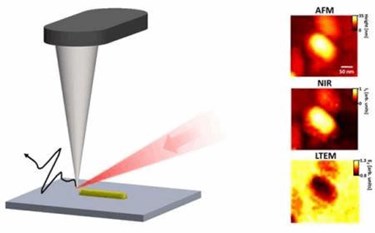
Researchers at Brown University have developed a modified method of laser terahertz emission microscopy (LTEM) to image, for the first time, individual nanostructures of materials being analyzed.
LTEM, which relies on acceleration of charge carriers in a material upon femtosecond excitation, typically is used to measure different properties of many types of materials, including integrated circuits and solar cells.
However, the comparatively larger wavelength of terahertz radiation (about 300 µm at 1 THz) limits its interaction with nanoscale structures.
“This is a well-known tool for studying essentially any material that absorbs light, but it’s never been possible to use it at the nanoscale,” said Daniel Mittleman, a professor in Brown’s School of Engineering, and co-author of the study. “Our work has improved the resolution of the technique so it can be used to characterize individual nanostructures.”
The new technique is based on “a scattering-type, near-field, tip-based approach” which consists of a metal pin with a tapered tip suspended over a sample material. When the sample is illuminated, the tip, which measures a few tens of nanometers across, captures a portion of the light to create an image of an individual gold nanorod with 20-nanometer resolution using terahertz emission — a thousandfold increase in resolution over previous LTEM imaging resolution of only a few tens of microns.
“Terahertz emission has been used to study lots of different materials — semiconductors, superconductors, wide-band-gap insulators, integrated circuits and others,” Mittleman said. “Being able to do this down to the level of individual nanostructures is a big deal.”
Mittleman and his colleagues at Brown are looking to apply their own technique to the analysis of perovskites — optically active, semiconducting compounds that are known to display intriguing electronic, light-emitting and chemical properties — which make them ideal for use in solar cells. The efficiency of the most advanced perovskite solar cells today tops out at 20 percent, though.
“One of the issues with perovskites is that they’re made of multi-crystalline grains, and the grain boundaries are what limits the transport of charge across a cell,” Mittleman said. “With the resolution we can achieve, we can map out each grain to see if different arrangements or orientations have an influence on charge mobility, which could help in optimizing the cells.”
Sponsored by the National Science Foundation, the study published in ACS Photonics, was led by Pernille Klarskov, a postdoctoral researcher in Mittleman’s lab, with Hyewon Kim and Vicki Colvin from Brown’s Department of Chemistry.
