Silicon Wafer Inspection With SWIR Cameras
Source: Raptor Photonics Limited

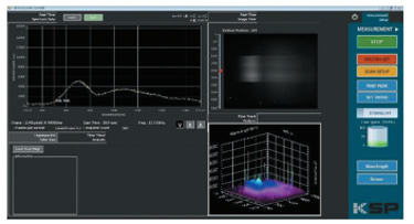
Silicon inspection can be a challenging problem for silicon and semi-conductor manufacturers in terms of pattern alignment, pattern defect inspection and edge position bonding inspection. During the manufacturing process, foreign particles and defects may appear on the top, bottom, inside or in between the wafers. It is important to find the location of these defects. Defects do not initially affect the chips functionality, but they do end up affecting the chips reliability. This article discusses the use of silicon wafer inspection with SWIR cameras.
access the Application Note!
Log In
Get unlimited access to:
Trend and Thought Leadership Articles

Case Studies & White Papers

Extensive Product Database

Members-Only Premium Content

Welcome Back! Please Log In to Continue.
X
Enter your credentials below to log in. Not yet a member of Photonics Online? Subscribe today.
Subscribe to Photonics Online
X
Subscribe to Photonics Online
