
Silicon Photonics Technology For Next-Gen Data Center Interconnects
By Johan Bauwelinck, IDLab; Gunther Roelkens, Photonics Research Group; Philippe Absil and Joris Van Campenhout, imec

Every day, we use a variety of internet services, including video streaming, web-browsing, social networking, e-mails and text messages, and cloud computing. Almost all these services run in data centers. According to Cisco Global Cloud Index, annual data center internet protocol (IP) traffic is expected to surpass 20 Zettabytes (or 20x1021 bytes) by 2021.
Inside these data centers, optical links connect the server racks through a complex network of fiber optical cable. Today, 100 Gb/s optical links — made up of 4x25 Gb/s single channels or lanes — sustain data traffic within the data center. These links transmit data over lengths of fiber stretching from a few meters up to 2km, with single mode fiber the optical medium of choice for spanning large distances.
Over the next few years, data center operators will upgrade their networks to 400 Gb/s optical links (by aggregating 4x100 Gb/s lanes per link) to cope with the exploding demand for data communication. Because the number of optical links within data centers will grow exponentially, these links need to be low cost and consume as little power as possible.
In parallel, the aggregate bandwidth to be handled by a single datacenter switch — which gears the information received on the input links to the appropriate output links in the datacenter fiber-optic network — will increase to 51.2 Tb/s from today’s 12.8 Tb/s. This capability demands ultra-high-density photonics transceiver technology, tightly integrated with the switch CMOS chip.
While pluggable electro-optical transceivers have been intensively used in the past, the industry has started to embrace co-packaged optics as a possible alternative, coupling the optics and switch CMOS chip in a single package. This approach greatly reduces the length of electrical lanes — from the centimeter to the millimeter range — leading to improved signal integrity and speed. Co-packaged optics also promise to enable significantly higher bandwidth density and lower power consumption, meeting the scaling requirements of next-generation data center interconnects.
Silicon Photonics: A Key Enabling Technology
Silicon photonics (SiPho) has been widely recognized as an attractive technology for integrating the essential building blocks of optical links. With this scalable technology, compact and low-power transceivers can be implemented at low cost and at high manufacturing volume by leveraging existing CMOS fabrication infrastructure.
Passive components (including fiber couplers, waveguides, and wavelength multiplexing filters) can be integrated together with active components (such as the electro-optic modulators, thermo-optic devices, and Ge-based photodetectors). Electronics circuits, such as drivers and trans-impedance amplifiers (TIA), can be fabricated on a separate wafer and assembled at the die level with the SiPho circuits using flip-chip assembly methods. In these circuits, the driver converts a standard CMOS bit state into an electrical voltage or current that is compatible with the optical device, while the TIA translates the photocurrent back into a standard CMOS bit state.
Imec, in collaboration with IDLab and the Photonics Research Group (the latter both are imec research labs at Ghent University) uses imec’s Si photonics platform on 200 mm and 300 mm SOI wafers — in combination with high-speed electronics — to develop the next generation SiPho interconnect technology.
The teams have achieved improvements at various levels of Si photonics technology development (i.e., process integration, individual component development, the sub-assembly level), bringing integrated solutions close to industrial implementation. This article discusses a few of the latest developments — some of which were presented at the 2019 European Conference on Optical Communication (ECOC) — in more detail.
Toward ultra-dense Tb/s co-packaged optics: a TSV-assisted hybrid FinFET CMOS-SiPho transceiver
Realizing ultra-dense Tb/s co-packaged optics is challenging for several reasons. First, the footprint of the SiPho transmitters and receivers must be sufficiently small. Second, the SiPho optical I/O module — essentially containing the modulator, photodetector, fiber coupler, driver, and TIA — needs to connect to the switch CMOS chip in the same package through high-density and high-speed electrical interconnects.
Therefore, high-speed electrical signals should be routed to and from the electro-optical transceiver array with low RF loss and high signal integrity. Traditionally, chip-to-package wire-bond interconnects combined with on-chip routing for RF and power/ground delivery have been used. But, for multi-Tb/s transceivers, this approach is unlikely to yield the required performance and density targets.
To enable high-speed electrical interconnections over short distances, researchers co-integrated 10-µm wide through-Si vias (TSVs) in a 100-µm-thick SiPho interposer, enabling substantially improved speed and electrical interconnect density compared to the wire-bond approach.
In this first-of-a-kind functional demonstrator, the TSVs route the electrical signals from the package to the 14 nm FinFET CMOS die, directly through the SiPho interposer. The FinFET chip, which is flip chipped on top of the SiPho interposer, contains the modulator driver and TIA arrays, which interface directly with the optical components in the SiPho interposer.
Although the TSVs were only used for low data-rate signals in this first demonstration, they have been shown to carry high frequency signals at 50 GHz and beyond with low RF loss in a separate measurement.
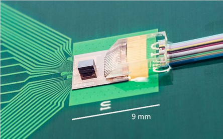
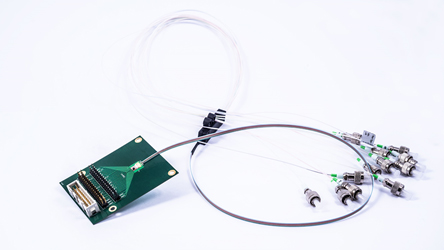
Fig. 1 — Photographs of the TSV-assisted FinFET CMOS-SiPho transceiver prototype (as presented at 2019 ECOC).
After hybrid assembly of the CMOS-SiPho optical module, a fiber array was attached and optically connected to the SiPho interposer using grating couplers.
On the transmit side of the photonics transceiver, each transmitter cell — implementing a 50Gb/s ring modulator — fits in a footprint of 100 µm x 100 µm. The receiver cells, with Ge photodetectors and TIA, cover a similar area. At a data rate of 40 Gb/s non-return to zero (NRZ), the transmitters and receivers operate with a dynamic power consumption of 0.16 pJ/bit and 0.08 pJ/bit, respectively.
In summary, the prototype demonstrated ultra-low power consumption with 1 Tbps/mm2 bandwidth density, paving the way to ultra-dense co-packaged optics in future datacenter switches.
Improved optical coupling: ultra-broadband low-loss single-mode fiber couplers
For applications requiring broadband optical coupling, edge couplers are preferred over grating couplers. These structures expand the optical mode diameter from sub-micron dimensions in the Si waveguides to the 10 µm mode-field diameter of a single-mode optical fiber. As such, they enable efficient and broadband coupling to fibers when those are butt coupled to the edge coupler through an optical facet etched in the SiPho chip.
When combined with mechanical alignment features also etched into the chip, high-throughput fiber packaging using passive alignment can be realized with the required sub-micron alignment accuracy. Such passive alignment can be beneficial over the current active alignment approaches, in which a laser needs to be coupled to the fiber array during the assembly process.
Researchers realized low-loss edge couplers with self-aligning V-grooves by adding a silicon nitride (SiN) waveguide layer to the SiPho platform. By properly etching the Si nitride layer, the optical mode can be expanded into a size that nearly matches that of the single mode fiber. A key step in this design is removal of the substrate below the buried oxide layer of the SOI wafer to prevent the expanded mode from leaking into the Si substrate.
The improved design resulted in a better than -1.5 dB/fiber coupling efficiency to single mode fibers for ultra-broadband operation in the O- and C-band. To facilitate passive and automated assembly of the fibers to the SiN edge couplers, self-aligned V-grooves have been developed on the chips.
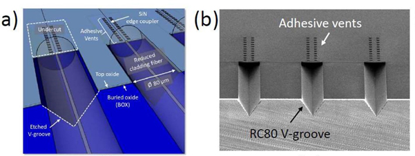
Fig. 2 — (a) Schematic and (b) SEM image of SiN edge couplers (as presented at 2019 ECOC).
Enhanced optical receiver sensitivity: Ge/Si avalanche photodetectors
To improve the power and reach performance of optical interconnects, optical engineers are always looking for ways to lower optical losses across the optical path. Besides directly lowering optical coupling losses, another option is to improve receiver sensitivity so the link can tolerate a higher optical loss.
To realize such sensitivity gains, avalanche photodiodes have received considerable attention from industry. In these diodes, an avalanche multiplication of holes or electrons — created by the initial electron-hole pairs generated by the absorbed photons — increases the gain of the diode. Such avalanche gain can help to improve both sensitivity and optical link margins, provided the additional noise generated in the process is sufficiently low.
Researchers have developed an avalanche photodiode with a separate absorption charge multiplication (SACM) region. In this diode, Ge is used as the absorption material and Si is used as the low-noise avalanche material. In contrast to conventional SACM designs, this solution has a lateral diode design with metal contacts only added to the Si region (and not to the Ge region). This results in enhanced primary responsivity and reduces manufacturing complexity.
The Ge/Si avalanche photodiode was fabricated using imec’s 200mm Si photonics platform. The diode features a high primary responsivity of 0.78 A/W at -2V, an avalanche multiplication gain larger than 8 and bandwidth of 32 GHz at -12V. Clear and wide-open eye diagrams at NRZ-OOK data rates of 25, 40, and 50 Gb/s show the potential of these avalanche photodiodes in improving receiver sensitivities and optical link margins at data rates of 40Gb/s and beyond.
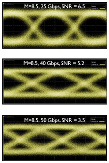
Fig. 3 — Electrical eye diagrams from the Ge/Si avalanche photodiode at 1550nm and -12V with NRZ-OOK data rates of 25Gb/s, 40Gb/s and 50Gb/s.
Low-power 106 Gb/s PAM-4 transmitter and receiver circuits for 400GbE interconnects
The capabilities of the electro-optical transceivers — in terms of speed, power consumption and footprint — can be significantly improved by combining the Si photonics building blocks with specialized high-speed, low-power electronics (e.g., drivers, TIAs, equalizers, and converters) and higher-order signal modulation formats.
Using this approach, 106 Gb/s low-power PAM-4 transmitters and receivers have been demonstrated. PAM-4 is the industry’s modulation format of choice for 100 Gb/s per lane transmission over 500 m. Then, 400 Gb/s data rates can be obtained by using four of these 100Gb/s lanes. In contrast to NRZ (a 2-level modulation format), PAM-4 is a four-level modulation format, with levels denoted as 00, 01, 10, and 11 (combining two bits in each level). While NRZ ideally switches between ‘all the light’ (1) or ‘no light’ (0), PAM-4 levels correspond to ‘no light,’ ‘one-third of the light,’ ‘two-thirds of the light,’ or ‘all the light’. Thus, with this 4-level format, the data rate can be doubled while keeping the same bandwidth.
Generating and receiving PAM-4 at line rates of 100 Gb/s has proven very challenging. In general, using a multi-level modulation format leads to reduced eye openings. On top of that, in a traditional single-modulator implementation, the modulator needs to have a linear transfer function. Most types of modulators, however, are non-linear devices. Attempts to solve this issue are mainly limited to the electrical domain and rely on power-hungry tools like digital signal processing (DSP) and equalization to compensate for any non-linearity.
A compact and low-power 106 Gb/s transmitter
To enable low-power 106Gb/s PAM-4 transmission, researchers proposed a transmitter topology based on the addition of two parallel 56 Gb/s NRZ electro-absorption modulators incorporated in a Mach-Zehnder interferometer. These modulators are then wire-bonded to a 55 nm SiGe BiCMOS driver.
Compared to a single-modulator solution, the transmitter generates the PAM-4 signal optically from the two EAMs without using any digital-to-analog converters (DACs) to go from bits to analog in the electrical domain. This setup completely removes the linearity requirement from the transmitter electronics and modulators, and requires no power-hungry equalization or DSP for compensation — leading to reduced complexity and much lower power consumption, as low as 1.5 pJ/b. Indeed, 106 Gb/s PAM-4 transmissions could be obtained over 1 km of single mode fiber with clear open eyes.
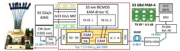
Fig. 4 — PAM-4 transmitter: architecture and experiment set-up (as presented at 2019 ECOC).
A sensitive and low power 106Gb/s receiver
Complementary to the transmitter, researchers demonstrated a sensitive and low-power 106Gb/s PAM-4 receiver. Like the transmitter, no power-hungry digital signal processing or equalization techniques were implemented in the receiver architecture or the test bed.
Key to the solution is the use of a low-noise, highly sensitive TIA. The gain and bandwidth settings of this TIA can be adjusted digitally in order to maintain good linearity for PAM-4 while preserving a high bandwidth. The TIA, implemented in 55 nm SiGe BiCMOS technology, is wire-bonded to a high-speed 50 GHz Si photonic Ge photodiode.
With a power consumption of only 1.51 pJ/b, a compact form factor and clear open eye diagrams at 106 Gb/s data rate over relevant fiber distances, this PAM-4 receiver meets all industrial requirements for 106Gb/s single-lane operation.
Conclusion
Si photonics technology solutions for next-generation datacenters have been demonstrated at different levels, including the process integration level (TSV-assisted hybrid FinFET CMOS-SiPho transceiver technology demonstrator), the component level (edge coupler designs and avalanche photodetector) and the sub-assembly level (PAM-4 transmitters and receivers). By efficiently co-integrating the individual Si photonics components with TSVs and with dedicated high-speed electronics, the demonstrated technology meets major industrial requirements, bringing this mature technology close to industrial implementation.
About the Authors
 Johan Bauwelinck is a professor in IDLab, an imec research group at Ghent University, where he is leading the Design lab. His research focuses on high-speed, high-frequency integrated circuits and systems for next generation transport, metro, access, datacenter and radio-over-fiber networks. He has promoted 21 PhDs and co-authored more than 300 publications and 10 patents in the field of high-speed electronics and fiber-optic communication. He is a member of the ECOC technical program committee.
 Gunther Roelkens is a full professor at the Photonics Research Group, an imec research group at Ghent University, where he is leading the work on silicon photonics high-speed optical transceivers and III-V-on-silicon heterogeneous integration. He has promoted 19 PhDs and co-authored more than 600 publications and 15 patents in the field of photonic integrated circuits. He received an ERC grant (MIRACLE) to start research in the field of mid-infrared photonic integrated circuits.
 Philippe Absil, PhD is the director of the 3D and Silicon Photonics technologies department at imec since 2013 and has been responsible for the silicon photonics technology platform development since 2010. Before that he spent seven years managing the advanced CMOS scaling program at imec. In the early 2000’s he developed the passive photonics platform technology for Little Optics Inc., Maryland, USA. He earned his PhD degree in 2000 from the department of electrical engineering of the University of Maryland at College Park, USA. His doctoral work contributed to the early demonstrations of semiconductor micro-ring resonators.
 Joris Van Campenhout is chief technologist silicon photonics and director of the Optical I/O industry-affiliation R&D program at imec, which covers the development of a scalable and industrially viable short-reach optical interconnect technology through silicon photonics. Prior to joining imec in 2010, he was a post-doctoral researcher at IBM’s TJ Watson Research Center (USA). He obtained a PhD degree in Electrical Engineering from Ghent University (Belgium) in 2007. Joris holds 7 patents and has authored or co-authored over 100 papers in the field of silicon integrated photonics, which have received 7000+ citations.