Quasi 2D Metasurface Coating Allows Waveguides To Be Smaller
By Jof Enriquez,
Follow me on Twitter @jofenriq

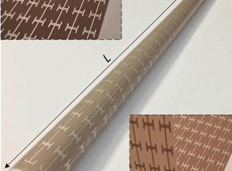
Researchers at Pennsylvania State University (Penn State) have developed a two-layer coating thin enough to be considered two-dimensional, which could allow further miniaturization of dielectric waveguides.
Controlling the various properties of metamaterials — such as mode confinement, polarization, scattering signature, and crosstalk, which are important in making metamaterials smaller — remains challenging for engineers. Existing techniques that depend on three-dimensional artificial cores or claddings, structural arrangement, geometric shape, and/or structural chirality, can achieve "highly confined modes, optical activity, or a low-scattering signature, but at the expense of increased propagation loss, form factor and weight," explain the authors of the study in an article published in Nature Communications.
To manipulate as many properties of optical waveguides as possible, without adding bulk and sacrificing versatility, Penn State researchers turned to using a two-layer coating to shrink the waveguides responsible in delivering the electromagnetic or optical signals.
"Imagine the water faucet in your home, which is an essential every-day device," said Douglas H. Werner, John L. and Genevieve H. McCain Chair Professor of Electrical Engineering. "Without pipes to carry the water from its source to the faucet, the device is worthless. It is the same with 'waveguides.' They carry electromagnetic or optical signals from the source to the device — an antenna or other microwave, millimeter-wave or terahertz device. Waveguides are an essential component in any electromagnetic or optical system, but they are often overlooked because much of the focus has been on the devices themselves and not the waveguides."
The quasi-2D coating, with each layer having near zero thickness and weight, is wrapped around a rod-shaped Teflon waveguide. The first layer designed to guide signals touches the Teflon surface of the waveguide, while the second one intended to cloak the waveguide is the outer layer.
According to the researchers, their coating minimizes the problematic crosstalk typically seen in conventional waveguides, whose bundles tend to leak signals that interfere with adjacent waveguides. Minimal crosstalk means engineers can make smaller waveguides, because the bundles can be situated nearer to each other.
"In terms of applications these would include millimeter-wave/terahertz/infrared systems for sensing, communications, and imaging that need to manipulate polarization, squeeze signals through waveguides with a smaller cross-section, and/or require dense deployment of interconnected components," said Zhi Hao Jiang, former postdoctoral fellow at Penn State and now a professor at Southeast University, Nanjing, China.
Werner, Jian, and Lei Kang, research associate in electrical engineering, Penn State, completed this research work through the Penn State Materials Research Science and Engineering Center, using funds provided by the National Science Foundation.
