
Photonic Soldering Reworks Printed Circuit Boards, Part I
 Lasers melt the solder around circuit board components to permit the removal of faulty components.
By: Erick Russell, ViTechnology
Contents
Hot air versus photonic soldering
System design
Temperature monitoring
Printed circuit board assembly consists of soldering components to a circuit board. Faulty components, once identified, must be replaced in a three-part rework process: the component is removed, the site is prepared for a new device, and a new component is attached. Engineers often use the rework process as a determining factor for board design—if a printed circuit board assembly can not be reworked (i.e. specific devices can not be replaced), it is often not considered manufacturable.
Continually shrinking package sizes and reduction of clearance areas available around components has made it increasingly difficult to rework and repair printed circuit board assemblies. Hand held electronics such as cell phones and pagers push the envelope of the board design criteria when rework and repair is considered.
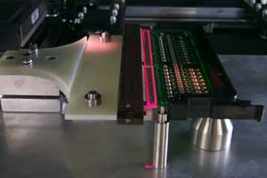
Increasingly tight process requirements and the growing complexity of printed circuit boards has prompted the development of photonic soldering, a new technology for selective soldering and rework (see Figure 1, at top). In photonic soldering, a laser source provides the energy to heat and reflow the solder. Scanning elements direct the beam in a precise pattern, and an optical pyrometer monitors the surface temperature of the components.
Laser soldering offers the advantages of inventive control tools and powerful computer interface for programming. The technology reduces the amount of tooling required for soldering different components, prevents the reflow of adjacent components, and increases the speed of which rework may be carried out.
Hot air versus photonic soldering
In traditional rework systems, components are removed by blowing hot air on the surface of the components, changing nozzles to match the perimeter of different sized components. A thermocouple monitors the hot air, which is controlled by microprocessor. After the solder has melted, an automated vacuum pickup system moves to the site and removes the component.
The hot air technique suffers from a number of disadvantages. These nozzles may cost hundreds of dollars, and require long lead times if customization is required. For components will small masses, the air may blow the component away from the site. Perhaps most important, the process time for this technique can take up to 15 minutes per component. In the fast paced electronics assembly environment, it is often more economical to throw out the board.
Photonic soldering has been a successful alternative to hot air convection soldering for applications that require precise process control and optimization of process time, and have physical constraints that prevent the use of shielding devices to protect adjacent components. Originally developed for personal computer assemblies, this technology has been well received by the telecommunications industry where the density of the component real estate is essential to the value of the final product. Using lasers to rework a component removes tooling costs and time required to refit the process for new components. By changing the path, speed, and intensity of the output beam, the laser can be reprogrammed for different components in a matter of minutes.
System design
The laser soldering system (ViTechnology; Haverhill, MA) incorporates a flashlamp-pumped neodymium-doped yttrium aluminum garnet (Nd:YAG) laser operating at 1064 nm as the energy source to melt the solder joints (<>
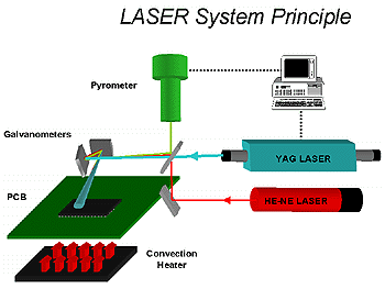
The laser is considered a Class IV system, and requires interlocks and shielding for operation. Once completely isolated, the laser downgrades to Class II; under normal operating procedures, no safety glasses or special facilities are necessary to operate the equipment. Such a system can be safely placed in a manufacturing environment.
The beam path is controlled by computer-controlled galvanometer, with separate reflectors used to direct the beam along the x- and y-axis. The devices are programmed for each component type and the paths are stored in the computer interface. The distance that the beam travels and the time it takes to complete the path can be programmed, allowing the operator to determine how rapidly the beam moves through the pattern. To show the path of the infrared Nd:YAG beam during the scan process, the beam of a red helium neon laser is positioned on the same optical path.
Temperature monitoring
In order to successfully remove or replace a component for rework. The YAG laser must be controlled to prevent overheating the components by applying too much heat too quickly. The goal is to simulate the thermal profile of a reflow oven, maintain thermal uniformity across the component, and prevent adjacent components from being over heated or reflowed.
To achieve these goals, the system incorporates an optical pyrometer to read the surface temperature of the component. The instrument assesses the 3.5 µm emission from the surface every 10 ms. The system compares this information with the set temperature of the programmed process parameters and adjusts the current as appropriate. Continuous process monitoring through a closed loop thermal regulation system ensures a repeatable and reliable process.
Part II of this article will discuss the use of photonic soldering in leaded device and area array device rework.
About the author…
Erick Russell is the laser systems product manager of Vision Inspection Technology, LLC, 179 Ward Hill Ave., Haverhill, MA. 01835. Tel: 978-372-1230; Fax: 978-372-1767; e-mail: Erussell@vitechnology.com.