Photodetector With Nanocavities Key To Smaller Optoelectronics
By Jof Enriquez,
Follow me on Twitter @jofenriq

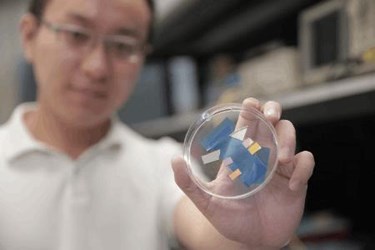
Researchers at the University of Wisconsin–Madison (UW-Madison) and the University at Buffalo (UB) have developed a very thin yet high-performance photodetector consisting of nanocavities sandwiched between a single-crystalline germanium and a reflective layer of silver. Fabricating the device shows it’s possible to shrink photoactive materials to the nanometer scale (<50 nm) without compromising their effectiveness.
Engineers miniaturizing optoelectronic devices to elevate performance have met two challenges as they try to shrink these next-generation electronics: one, “amorphous” thin-film materials tend to lose their quality and, two, ultrathin materials become almost transparent, and as a result, they lose the ability to absorb photons.
Electrical engineering professors Zhenqiang (Jack) Ma and Zongfu Yu at UW–Madison, as well as Qiaoqiang Gan at UB, built a single-crystalline germanium nanomembrane photodetector device that surmounts the aforementioned hurdles to further improving optoelectronic performance. The researchers assembled the device by utilizing a unique fabrication method, integrating conventional bulk semiconductor wafers, such as silicon and germanium, to realize single-crystalline films on foreign substrates.
Semiconducting materials such as germanium lack the atomic structure — the regular, repeating order of a crystal — ideal for smaller optoelectronic applications. However, the researchers used a nanocavity interference mechanism to enhance and circulate the light absorbed by the material.
“The idea, basically, is you want to use a very thin material to realize the same function of devices in which you need to use a very thick material,” says Ma. “Because of the nano-cavities, the photons are ‘recycled’ so light absorption is substantially increased — even in very thin layers of material.”
The nanocavities of the new photodetector can be tuned to absorb specific light wavelengths, and to exhibit unique optoelectronic properties, such as the strong field effect and spectral selectivity.
This advance in optoelectronic technology makes it more feasible than ever to shrink industrial and consumer electronics without sacrificing performance.
“We’ve created an exceptionally small and extraordinarily powerful device that converts light into energy,” says Gan, associate professor of electrical engineering in UB’s School of Engineering and Applied Sciences. “The potential applications are exciting because it could be used to produce everything from more efficient solar panels to more powerful optical fibers.”
