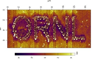
ORNL Microscopy Pencils Patterns In Polymers At The Nanoscale

Scientists at the Department of Energy’s Oak Ridge National Laboratory have used advanced microscopy to carve out nanoscale designs on the surface of a new class of ionic polymer materials for the first time. The study provides new evidence that atomic force microscopy, or AFM, could be used to precisely fabricate materials needed for increasingly smaller devices.
Polymerized ionic liquids have potential applications in technologies such as lithium batteries, transistors and solar cells because of their high ionic conductivity and unique structure. But many aspects of the recently discovered materials are still not well understood.
When ORNL researchers used an atomic force microscope to begin characterizing the properties of polymerized ionic liquid thin films, the experiment yielded some surprising results.
“We were expecting to measure ionic conductivity, and instead we found that we were forming holes on the surface,” said ORNL’s Vera Bocharova, corresponding author on the study published in Advanced Functional Materials. “Then we started to think about how this might have great applications in nanofabrication.”
Nanolithography is the dominant technique used by industry for nanofabrication, but its size limitations are leading researchers to explore other methods such as AFM.
“This study is part of our search for alternative methods and materials that can be used to create smaller sized objects,” Bocharova said. “For example, our technique might be interesting for the miniaturization of semiconductor technology.”
Similar AFM techniques have been used to study and produce patterns in nonconductive polymers, but the ORNL study uncovered several differences in the application to polymerized ionic liquids.
“In comparison to nonconductive polymers, we have to apply less bias — four volts instead of 20 volts — to generate the holes, which is good in terms of energy savings for future applications,” Bocharova said.
In nonconductive polymers, the high voltage applied through the AFM tip punctures the material’s surface by localized heating. In contrast, the ORNL team used experiment and theory to determine that the holes formed in the conductive polymer liquids resulted from negative ions migrating to the positively charged microscope tip. The researchers plan to continue refining the technique’s capabilities and their understanding of the polymerized ionic liquids’ properties.
“Right now the size of the formed features is in the range of 100 nanometers, but it’s not the limit,” Bocharova said. “We believe it’s possible to change the experimental setup to advance to lower scales.”
The paper is published as “Controlled Nanopatterning of a Polymerized Ionic Liquid in a Strong Electric Field.” Coauthors are ORNL’s Vera Bocharova, Alexander Agapov, Alexander Tselev, Rajeev Kumar, Alexander Kisliuk, Ivan Kravchenko, Bobby Sumpter, Alexei Sokolov, Sergei Kalinin, and Evgheni Strelcov; Liam Collins of the University College Dublin; and Stefan Berdzinski and Veronika Strehmel of the Hochschule Niederrhein University of Applied Sciences. Sokolov holds an ORNL-University of Tennessee Governor’s Chair appointment.
This research was supported by ORNL’s Laboratory Directed Research and Development program and was conducted in part at ORNL’s Center for Nanophase Materials Sciences, a DOE Office of Science User Facility. Parts of the research were supported by DOE’s Office of Science and the National Science Foundation.
ORNL is managed by UT-Battelle for the Department of Energy's Office of Science. DOE's Office of Science is the single largest supporter of basic research in the physical sciences in the United States, and is working to address some of the most pressing challenges of our time. For more information, visit http://science.energy.gov.
Source: Oak Ridge National Laboratory
