
Near field holography replicates gratings in integrated optical components

By: Laurie Toupin
Near field holography (NFH) technology can provide a practical, economical volume manufacturing technique for nanometer-sized integrated optics in indium phosphide (InP) substrates, say engineers at Denmark-based ADC, who adapted the method to manufacture gratings and waveguides for distributed feedback (DFB) lasers and other grating-based applications.
To produce nanometer-scale structures, a company must use either electron-beam (e-beam) writing or direct holography techniques, says Kristian Buchwald, ADC product manager for phase masks. E-beam equipment is slow and expensive, while the direct holography is labor intensive. Both methods are high maintenance.
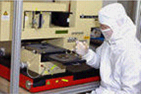
The ADC NFH manufacturing process is not only low maintenance, but also extremely reliable, says ADC's Dirk Jessen. The three basic components for this technique include a mask aligner, a phase mask for printing, and the NFH technology.
How it works
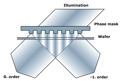
Near field holography, similar to lithography, uses a phase mask to print gratings into planar structures. The mask gratings consist of well-defined grooves etched into a quartz substrate.
If linearly polarized, monochromatic, collimated light is incident on the grating at the Bragg angle, the zeroth order will just pass through the mask without being affected. The grating parameters can, however, be designed so that a –1 diffracted order with the same intensity as the zeroth order will be radiated at an identical but opposite angle from the zeroth order (see Figure 2). The interference of the two beams form a standing wave pattern below the mask grating which extends a few microns downward from the mask. A resist layer on a wafer, exposed by that standing wave, leads to a replicated grating in photoresist. For DFB laser applications, this resist grating is then transferred into InP to yield the desired optical grating.
System design
A mask aligner from Karl Suss (Munich) with a special NFH option helps keep the 100-nm structures in place. "The mask aligner is well known in the semiconductor industry and it is very production oriented," says Buchwald.
A standard ultraviolet (UV) mercury lamp serves as the illumination source. This method is very forgiving as to the exact incidence angle of the exposure beam as well as to monochromacy and parallelity of the light, says Buchwald. "Using a conventional mercury lamp translates into low upkeep."
ADC engineers suggested both system and process optimization changes to adapt the NFH technology for manufacturing. For example, they had to increase the normally low coherence length of the mercury lamp, to a longer proprietary value required by the NFH process.
Also, due to the reflection of the indium phosphate (InP), a primary wafer material for DFB lasers, Newton rings appeared in the wafer after production. ADC engineers devised a method for reducing the reflection in order to eliminate the rings.
The degree of volume production the process can accomplish depends largely on the types of materials used and the number of layers required. On the average, Jessen estimates that the process throughput is about 20 InP wafers per hour.
ADC researchers demonstrate the NFH process to customers on standard InP wafers at their Denmark facility. They will perform a preliminary optimization and viability study on a manufacturer's wafers for a charge. Soon they plan to offer recipe packages that will consist of further optimization on customer wafers and a customer specific disclosure of optimization parameters relevant to their specific wafers.
"There is a great need for the NFH process because there is a tremendous growth in the DFB laser market and the present manufacturers are wondering how to keep up," says Jessen. The NFH process will provide an economical solution to the problem.
About the author…
Laurie Toupin is a freelance science writer based in Massachusetts.