
Molded microlens technology enhances cell phone backlighting

Computer-based design and fabrication techniques yield enhanced lightguides that render LED emission uniform with minimal loss.
By: Brad Lizotte, Lumitex Inc.
Developing compact LCD backlights for devices such as cell phones, PDAs, or portable medical devices forces the engineer to address multiple design considerations, including lighting uniformity, type and number of light-emitting diodes (LEDs), emission direction (top or side firing), as well as the addition of alignment features to enhance manufacturability.
The design cycle for such displays devotes a significant amount of time to achieve acceptable lighting output and uniformity. Up until now, technologies for ensuring uniformity have incorporated imprecise chemical and laser-etch processes to develop optical patterns for light guides. Etched onto the surface of a metal mold insert, the patterns are impressed on polycarbonate or other materials, transferring light extraction features to the light guide.
Laser and chemical etching, though improved in recent years, are at best imprecise methods that rely more on multiple iterations and luck than a controlled production process. A computer-controlled approach to molded plastic microlens arrays (Lumitex Inc.; Strongsville, Ohio) offers a controllable, design-compatible solution to deliver a backlight that minimizes the number of LEDs required for an application, providing attendant power and cost savings. Very precise and controlled features are applied to a molded insert using a proprietary machining technique. During the molding process, these precision features are transferred to the final molded lightguide.
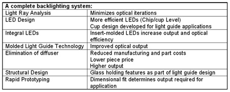
Backlighting designs
In current cell phone designs, the lightguide is either combined with chip-on-glass (COG) or chip-on-flex (COF) LCDs that mount the drive circuitry directly to the display glass, or is attached to a flex circuit that is, in turn, mounted to the glass. The integrated approach significantly reduces overall space requirements for the LCD module.
A typical cellular phone display requires four to six yellow-green LEDs to backlight a viewing area of 30 mm X 30 mm to brightness levels of approximately 0.5 fL (1.7 cd/m2) at the face of the LCD, with total current typically 48 to 120 mA. Even using conventional light guide technology to direct and diffuse the illumination, recently developed high brightness LEDs offer the handset designer the option of lighting displays with as few as two or three emitters. (see Audio Interview: Bob Steele on high brightness LEDs )
The light guide technology improves backlight conditioning to the point that cellular LCDs can be backlit with as few as one of the new high efficiency LEDs, or two of the more commonly used and lower efficiency yellow-green LEDs.

Fabricating molded microlens features
The molded light extraction technology uses up to 30,000 miniature lenses/in2 in the rear surface of the lightguide to diffuse and direct LED illumination (see Figure 1). Each feature varies in depth and other variables to extract light at the precise amount required by its location in the lightguide to achieve optimal uniformity. Because of the volume of features and the light distribution characteristics, the approach eliminates the need for a diffuser in many applications.

The key to the efficiency of this technology is precision control of all light extraction features, which have been designed for maximum optical efficiency focusing a very high percentage of the available light from the LEDs to the front face of the lightguide.
The size, shape, population, depth and location of each light-extracting feature are precision engineered in the molded light guide and manufactured to tolerances much less than 25 µm. The design of every feature must be tailored to account for the type of light source package used as well as its output distribution, location, position, and orientation.
The features are introduced into the mold tooling via custom metal inserts. Once the optical characteristics of a part are approved, the insert's precise optical pattern is duplicated to the remaining mold inserts with highly consistent results. With other processes, light extraction features are created using laser machining or chemical etch profiling to mold inserts. These methods typically require multiple iterations, with inconsistent results, even after a "successful" laser or chemical etch pattern is developed. Subsequent optical mold inserts depend more on art than science and are difficult to duplicateprocess variations and inconsistencies result from cavity to cavity when multiple mold tools are required.
This microlens process combines high resolution, optical ray trace analysis, precision molded light extraction and precision design translation from the virtual model to final production in a process that is under complete control.
Designing the array
Using a customized ray analysis package, the LED to be used is characterized for output and introduced into a virtual three-dimensional model of the part design
The results of this analysis are used in conjunction with proprietary software developed by Lumitex to produce command files which are directly used in the fabrication process. The first iteration of the part establishes a performance baseline, so that subsequent part iterations are made based on a known optical performance with a controlled progression.
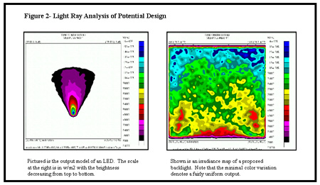
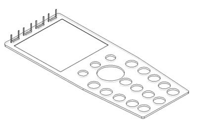
The process allows the optical features of the molded light guide to be rotated so that they are directly oriented to the optical path of the LED's individual light rays, enhancing the efficiency and optical performance of the system. In the case of high-brightness LEDs, this approach can reduce the total number of LEDs required to as few as one, cutting costs and simplifying assembly (see Figure 3).
Application-specific LEDs
A custom LED specifically developed for display backlighting applications further improves performance. Many backlights use LEDs with two chips that predetermine light location. Here, however, the LED allows the light source to be located where it is most optimal, including angular locations. More importantly the 2-chip LEDs often require 4.4 nominal VDC versus the 2.2 VDC single chip LED required by this new molded light guide technologyan important decrease when you consider that today's wireless handset power amplifiers have outputs of 3.6 VDC. LEDs with 4.4 VDC operating voltage may require power management components and the related issues that go with them. Now, that can be avoided entirely.
These LEDs also have a custom reflector design that optimizes the shape of the light output for increased efficiency in light pipe applications. They also accept the current, commercially available chip technology.
Using molded light guide technology as a structural aspect of display design permits complete integration of the display package. This, coupled with the improved performance of LEDs and the reduced complexity of COG and COF LCD designs, permits lower part counts (fewer LEDs), a substantial reduction in the amount of space required, and overall improved output at lower power levels.
About the author…
Brad Lizotte is Sales & Marketing Manager with Lumitex Inc., Strongsville, Ohio. Phone: 440-243-8401; fax: 440-243-8402; e-mail: blizotte@lumitex.com.