MIPT Physicists Develop Ultrasensitive Nanomechanical Biosensor

Two young researchers working at the MIPT Laboratory of Nanooptics and Plasmonics, Dmitry Fedyanin and Yury Stebunov, have developed an ultracompact highly sensitive nanomechanical sensor for analyzing the chemical composition of substances and detecting biological objects, such as viral disease markers, which appear when the immune system responds to incurable or hard-to-cure diseases, including HIV, hepatitis, herpes, and many others. The sensor will enable doctors to identify tumor markers, whose presence in the body signals the emergence and growth of cancerous tumors.
The sensitivity of the new device is best characterized by one key feature: according to its developers, the sensor can track changes of just a few kilodaltons in the mass of a cantilever in real time. One Dalton is roughly the mass of a proton or neutron, and several thousand Daltons are the mass of individual proteins and DNA molecules. So the new optical sensor will allow for diagnosing diseases long before they can be detected by any other method, which will pave the way for a new-generation of diagnostics.
The device, described in an article published in the journal Scientific Reports, is an optical or, more precisely, optomechanical chip. “We’ve been following the progress made in the development of micro- and nanomechanical biosensors for quite a while now and can say that no one has been able to introduce a simple and scalable technology for parallel monitoring that would be ready to use outside a laboratory. So our goal was not only to achieve the high sensitivity of the sensor and make it compact, but also make it scalabile and compatibile with standard microelectronics technologies,” the researchers said.
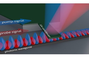
Unlike similar devices, the new sensor has no complex junctions and can be produced through a standard CMOS process technology used in microelectronics. The sensor doesn’t have a single circuit, and its design is very simple. It consists of two parts: a photonic (or plasmonic) nanowave guide to control the optical signal, and a cantilever hanging over the waveguide.
A cantilever, or beam, is a long and thin strip of microscopic dimensions (5 micrometers long, 1 micrometer wide and 90 nanometers thick), connected tightly to a chip. To get an idea how it works, imagine you press one end of a ruler tightly to the edge of a table and allow the other end to hang freely in the air. If you touch the latter with your other hand and then take your hand away, the ruler will start making mechanical oscillations at a certain frequency. That’s how the cantilever works. The difference between the oscillations of the ruler and the cantilever is only the frequency, which depends on the materials and geometry: while the ruler oscillates at several tens of hertz, the frequency of the cantilever’s oscillations is measured in megahertz. In other words, it makes a few million oscillations per second!
There are two optical signals going through the waveguide during oscillations: the first one sets the cantilever in motion, and the second one allows for reading the signal containing information about the movement. The inhomogeneous electromagnetic field of the control signal’s optical mode transmits a dipole moment to the cantilever, impacting the dipole at the same time so that the cantilever starts to oscillate.
The sinusoidally modulated control signal makes the cantilever oscillate at an amplitude of up to 20 nanometers. The oscillations determine the parameters of the second signal, the output power of which depends on the cantilever’s position.
The highly localized optical modes of nanowave guides, which create a strong electric field intensity gradient, are key to inducing cantilever oscillations. Because the changes of the electromagnetic field in such systems are measured in tens of nanometers, researchers use the term “nanophotonics” – so the prefix “nano” is not used here just as a fad! Without the nanoscale waveguide and the cantilever, the chip simply wouldn’t work. Abig cantilever cannot be made to oscillate by freely propagating light, and the effects of chemical changes to its surface on the oscillation frequency would be less noticeable..
Cantilever oscillations make it possible to determine the chemical composition of the environment in which the chip is placed. That’s because the frequency of mechanical vibrations depends not only on the materials’ dimensions and properties, but also on the mass of the oscillatory system, which changes during a chemical reaction between the cantilever and the environment. By placing different reagents on the cantilever, researchers make it react with specific substances or even biological objects. If you place antibodies to certain viruses on the cantilever, it’ll capture the viral particles in the analyzed environment. Oscillations will occur at a lower or higher amplitude depending on the virus or the layer of chemically reactive substances on the cantilever, and the electromagnetic wave passing through the waveguide will be dispersed by the cantilever differently, which can be seen in the changes of the intensity of the readout signal.
Calculations done by the researchers showed that the new sensor will combine high sensitivity with a comparative ease of production and miniature dimensions, allowing it to be used in all portable devices, such as smartphones, wearable electronics, etc. One chip, several millimeters in size, will be able to accommodate several thousand such sensors, configured to detect different particles or molecules. The price, thanks to the simplicity of the design, will most likely depend on the number of sensors, being much more affordable than its competitors.
Source: Moscow Institute of Physics and Technology
