
MEMS Technology Grabs The Telecom Spotlight
Contents
Size determines complexity
Moving from n2 to 2n
Foundry for hire
In the lab
Editor's Report
Once a laboratory curiosity, micro-electro-mechanical systems (MEMS) technology has come into its own, dominating the recent Optical Fiber Communications Conference (OFC '00; Baltimore, MD; March 5-10) with switching applications (see OFC 2000: Optical Switching Systems Stir Up Wavelength Management Debate).
Three start-ups made headlines during the conference: Sunnyvale, CA-based Xros Inc. (pronounced Chi-ros, as in the Greek letter chi), Optical Micro-Machines (San Diego), and Cronos (Research Triangle Park, NC). Meanwhile, Lucent showcased its LambdaRouter, announced in October at Telecon '99 (Geneva).
Industry watchers have since seen the photonics foodchain in action, with Nortel Networks snapping up Xros almost immediately after the conference (see Nortel Steps Into MEMS Switching With Xros Acquisition), and JDS Uniphase (San Jose, CA) nabbing Cronos shortly after (see JDS Uniphase to Acquire Optical MEMS Shop Cronos for $750 Million). Only Optical Micro-Machines still stands alone, having announced technology trials with Siemens, but no other liasons as yet.
Size determines complexity
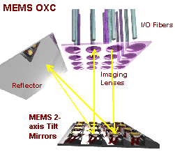
There are two main types of MEMS switch configurations: 2n architecture, and n2 architecture. In 2n architecture, two opposing arrays of n micromirrors face one another. An input beam reflects from a mirror on the first array to any other mirror on the second array, which steers it to the appropriate output fiber.
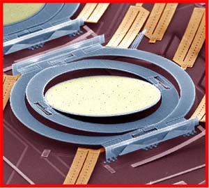
For example, Lucent's 256 input Lambda-Router consists of two opposing 16 x 16 element arrays of micromirrors (see Figure 2). Fabricated on a 1 mm pitch, each 0.5-mm-diameter mirror can rotate along two distinct axes, with better than 0.01° accuracy, allowing each mirror in one array to direct an incident beam to any other mirror in the opposing array. In other words the device can route a beam from one of 256 input fibers to any one of 256 output fibers.
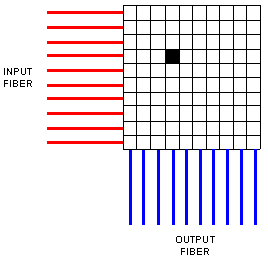
The 2n architecture, offers advantages over n2 designs in which all 256 input fibers would connect to the switching matrix on one axis and the 256 output fibers attach on an orthogonal axis, for a total of 65536 micromirrors (see Figure 3). According to Lucent's David Bishop, who leads the MEMS research effort at the company, 2n architecture possesses a clear advantage for large switching fabrics. To produce an n2 switch for 1024 inputs and outputs, for example, requires the fabrication of more than a million switching elements, whereas a 2n switch only requires a pair of 32 x 32 element arrays.
Moreover, if a switching pixel malfunctions, it effectively blocks the ability of the switch to route the signal from a given input to a given output, creating a potential need for redundancy of entire rows of switch elements. In the case of 2n architectures, if a mirror malfunctions, any other mirror in the array can route that same signal. The need for redundancy still exists, but on a 2n level, not on an n2°level. When you consider that proponents of large switching fabrics are talking about 1000 x 1000 arrays on a volume production level, the advantage of 2n architecture becomes clear.
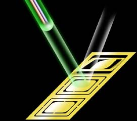
Nortel acquisition Xros also specializes in a 2n switch, touting a prototype consisting of two 36 x 32 arrays of 2 mm x 2 mm mirrors that can switch as many as 1152 inputs to 1152 separate outputs (see Figure 4). Built from single-crystal silicon, the devices are manufactured by undercutting rather than by deposition. The rectangular, gold-coated mirrors are mounted on torsion hinges; piezo-electric-based flexure sensors on the mirrors monitor position to provide accuracy on the order of 1 µrad.
According to Xros president Greg Reznick, the company is working on the prototype now, with trial units planned for summer.
Moving from n2 to 2n
Switching contender Optical Micro Machines is currently working with an n2 architecture for switches up to 32 x 32 arrays. Rather than providing analog control about multiple axes, the mirrors are binary—either on (routing a signal to a predefined output) or off.
While touting the robustness and performance of the smaller switches, company president and CEO Hus Tigli agrees that the n2 approach has its limitations and that the 2n approach is best for large switching fabrics. "Absolutely, you'd have to do it, otherwise the number of mirrors would get out of hand. We're working on 3-D [2n] architecture with analog scanning mirrors. Rather than being either on or off, each micromirror has intermediate positions, can tilt on two axes." The configuration appears to be similar to that pursued by both Lucent and Xros.
For now, though, OMM is enjoying considerable success with its n2 design, featured at OFC. Not only was the switch showcased by Siemens in a demo network at CeBIT 2000, the National Transparent Optical Network Consortium has been routing live traffic over a sample switch in an unmanned Oakland, CA central office. "Additionally, we were able to re-provision the optical switching network from a remote location," noted Robert Hendrickson, director of the advanced technologies laboratories at GST Telecom, and a project member.
According to Tigli, the company is slated to begin volume production in the summer. OMM does not have its own foundry, but farms out its MEMS fabrication to outside suppliers that Tigli declined to name. He appeared unconcerned with the JDS Uniphase acquisition of Cronos, however.
When queried about his own company's future as a solo entity, Tigli was sanguine. "This is an intensely attractive field," he said, noting the recent acquisitions, but maintaining that OMM will go its own way for the foreseeable future. "We believe the best destiny for the company is to be an independent switch subsystem supplier," he said. "There's plenty of action in this field." Time will tell. It will be interesting to see if this prediction plays out, or if OMM indeed becomes a jewel in some other telecom crown.
Foundry for hire
Unlike the other commercial players in the space, Cronos has previously positioned itself as technology-centric rather than product-centric. The pitch was that given a MEMS concept, Cronos would provide the design and the manufacturing pieces of the puzzle, producing a prototype in 9-13 weeks (see Microcosm, Cronos Team for MEMS Design Kit). Nanovation, for example, has taken advantage of Cronos' offerings to produce its switch offerings. Although the JDS Uniphase deal may change that agreement in future, at present the arrangement between the two companies remains in place.
JDS Uniphase currently produces both optomechanical and polymer-based switches. The Cronos acquisition will allow it to offer MEMS-based optical switches in the future.
In the lab
So much for the blur of commercial activity in the MEMS field. Work continues in the laboratory, also, with researchers broadening the application of the technology. MEMS has applications in smaller switching fabrics also, as demonstrated by Martin Hoffman and colleagues at the Universität Dortmund (Dortmund, Germany).1 The group used U-shaped lateral MEMS actuators to mechanically shift an input fiber held in a V-groove from one output fiber to another, and a micromachined clamp to hold the fibers in position when switching was not taking place (see Figure 5). Thin film heaters generate a controlled expansion in the silicon to result in displacements as large as 200 µm without angular offset, allowing the group to realize 1 x 4 optical switches.
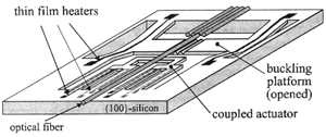
The devices demonstrated insertion loss of less than 1 dB and switching times on the order of 400 ms. Switching power ranged from 800 mW for a 1 x 2 design to 1500 mW for a 1 x 4 design. Crosstalk was less than –60 dB.
Nabeel Riza and colleagues at the University of Central Florida's Center for Research and Education in Optics and Lasers (CREOL; Orlando, FL) have developed a variable optical attenuator based on the Texas Instruments digital multimirror device, a binary MEMS structure that either reflects full power or partial power to a gradient index lens output port, depending on deflection of the electrostatically-controlled micromirror.2 The device can operate at speeds on the order of microseconds, and provide up to 37.8 dB of optical attenuation.
Lih Lin and collaborators at AT&T Labs-Research (Red Bank, NJ) are working on MEMS devices for polarization mode dispersion (PMD) control, and Christi Madsen and others at Lucent Technologies Bell Labs (Murray Hill, NJ) have developed a MEMS prototype that dynamically compensates for chromatic dispersion. Look for details on both of these projects in forthcoming articles on PMD and dispersion compensation.
References
1. M. Hoffman, et. al., "Lensless Latching-Type Fiber Switches Using Silicon Micromachined Actuators," OFC 2000 Technical Digest, paper #ThQ5, Baltimore (2000).
2. S. Sumriddetchkajorn and N. Riza, "Micromachine-based Fault-Tolerant High Resolution High-Speed Programmable Fiber-Optic Attenuator," OFC 2000 Technical Digest, paper #ThQ1, Baltimore (2000).
By: Kristin Lewotsky, Editor, Photonics Online