Making Flat Optical Lenses By Stacking Metasurfaces
By Jof Enriquez,
Follow me on Twitter @jofenriq

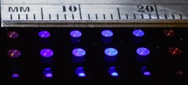
Engineers at California Institute of Technology (Caltech) have successfully demonstrated how to stack metasurfaces to form flat optical lenses that can be mass-produced and integrated with electronics and image sensors.
Conventional optical systems consist of optical components assembled to tight alignment specifications, a task that is increasingly more challenging as demand for miniaturized consumer electronics, wearables, and medical devices rises.
As an alternative, metasurfaces – extremely thin films of "metamaterials," or assemblies that contain features, patterns, or elements that enable unprecedented control of light – could accelerate the development of more advanced, yet low-cost, optical technologies.
"The main advantage of metasurfaces stems from the capability to make sophisticated planar optical systems composed of lithographically stacked electronic and metasurface layers. The resulting optical system is aligned lithographically, thus eliminating the need for post-fabrication alignments," explain the Caltech researchers in Nature Communications.
To demonstrate this new optical system, they fabricated a miniature flat camera integrating a monolithic metasurface lens doublet, corrected for monochromatic aberrations, and an image sensor.
"The doublet lens, which acts as a fisheye photographic objective, has a small f-number of 0.9, an angle-of-view larger than 60° × 60°, and operates at 850 nm wavelength with 70% focusing efficiency. The camera exhibits nearly diffraction-limited image quality, which indicates the potential of this technology in the development of optical systems for microscopy, photography, and computer vision," the engineers write in a recent online issue of the journal.
A classical lens made of plastic or glass has a curved shape that bends the path of incoming light toward a single focal point.
In comparison, Caltech's flat lenses, created by combining two layers of metamaterial studded with tens of millions of silicon nanoposts or nanopillars, accomplish the same task through tiny cylinders with dimensions of just 600 nanometers tall, and with varying diameters in the hundreds of nanometers. Controlling the width of the nanoposts allows the engineers to finely adjust the path of light passing through the metasurface to create flat lenses.
"The way we make lenses hasn't changed much since the time of van Leeuwenhoek. Until now," says Caltech's Andrei Faraon in a news release. He was referring to Dutch scientist and lens-maker Antonie van Leeuwenhoek, who created some of the first microscopes.
Faraon, an assistant professor of applied physics and materials science in Caltech's Division of Engineering and Applied Science, collaborated with Caltech postdoctoral researcher Amir Arbabi and Seunghoon Han from Samsung Electronics, as well as Caltech graduate students Seyedeh Mahsa Kamali and Yu Horie, in developing the flat lens system.
"Metasurfaces like these can be easily mass produced, much the way computer chips are," says Arbabi. "That means this could be a cheap and easily scalable way to create tiny lenses just a few millimeters in diameter."
The Caltech team claims their flat lenses could be seamlessly integrated with CMOS (complementary metal-oxide semiconductor) image sensors, microscopes, and medical devices such as endoscopes. They are collaborating with NASA's Jet Propulsion Laboratory and industrial partners to create metasurfaces for use in commercial devices such as miniature cameras and spectrometers.
