
Laser Direct Imaging Brings Flexible Manufacturing to Printed Circuit Industry

By: John Post Wheeler
As an alternative to conventional contact processes for printed circuit board manufacturing, laser direct imaging (LDI) cuts a significant amount of time from the fabrication process by eliminating the need for photomasks to pattern photoresist. Attempts to commercialize LDI systems began as early as 1970, but until recently, the technology has been unable to compete with traditional photographic processes. Now, manufacturers such as Etec Systems Inc. (Tucson, AZ) are releasing LDI units that provide a cost-effective alternative to traditional processes, especially for short-run high-end boards, where quick-change flexibility and rapid turnaround are critical.
From CAD to resist
For most of its life, printed circuit manufacturing has been tied to the traditional contact print process. In contact lithography, a photographic mask called a phototool is generated from a drawing and placed on a resist-covered panel. The resist is exposed by a conventional light source, then developed, and the panel is etched. Generating the phototool itself is a time-consuming, multistep process, but in the manufacturing process, automated exposure systems combined with a 5 s exposure time can produce up to 150 panels per hour.
LDI, on the other hand, goes directly from a CAD drawing to exposure of the resist, completely eliminating the mask-making steps, along with the yield loss associated with that process (see Figure 1). Since the data are stored digitally, changing from one design to another is quick and easy. According to Matt Kesler, product manager of the Interconnect Products Group for Etec, total cycle time, from design to finished interconnect, can be significantly less than that required for contact printing.
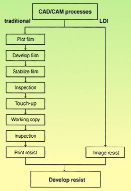
Etec's DigiRite 2000 exposes a standard 24-in. plate in approximately 50 s; throughput, including download, setup, and parts-handling time, is typically from 30 to 40 plates per hour. Cycle time for short and medium runs can be reduced by 80% or better over contact printing, because the time needed to fabricate, inspect, and touch up the mask is eliminated.
How it works
The system uses a high-power argon-ion laser, operating in the ultraviolet, as its light source. An optical system incorporating reflective optics and specially designed ultraviolet achromatic lenses allows the system to operate at multiple wavelengths (351 to 364 nm) and maintain a focused spot size of ±12.7 µm (FWHM). A granite base provides structural rigidity and thermal stability.
In operation, the laser beam is split into multiple, independently-addressable segments and scanned over a 6-in. width by a rotating polygon. A precision air-bearing stage moves the panel longitudinally to create a 6-in. x 24-in. stripe. The table is then indexed horizontally and the process repeated. Maximum total scan area is 30 in. x 24 in. Absolute positional accuracy is ±12.7 µm with ±5 µm repeatability.

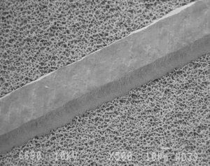
When a substrate is loaded, the LDI system automatically adjusts the height to compensate for board thickness and aligns and levels the substrate for a best plane fit to compensate for any thickness variation in the panel. During operation, the system continually monitors and corrects spot location to accommodate for normal variations in the system environment. A scanning electron microscope (SEM) image of features produced by the system is shown in figure 3. According to Kesler, the minimum feature size produced by the DigiRite 2000 is 50 µm, but the technology is compatible with features of 25 µm or less.
Kerry Grimes, president of GDI Inc., a distributor of dry photoresist materials for the printed circuit industry, believes that LDI systems will become a major factor in circuit card manufacturing. "With the focus on small lots, JIT purchasing, and rapid changeover, the ability to take an order for a 10-layer interconnect board and deliver it within 24 hours will command a significant premium." This sentiment was echoed by Jyrik Ylatalo from Aspocomp, a printed circuit manufacturer in Finland, who recently purchased a DigiRite 2000 system. "The higher yield and reduced cycle time...will give us an important advantage over the competition, which is still using conventional imaging techniques."
About the author...
John Post Wheeler is a freelance writer specializing in science and technology.