
Ink jet printer produces full-color, video-rate OLED display

Editor's Report
Displays manufactured from organic light-emitting diodes (OLEDs) are the hot story right now in the industry (see DappCon '00: OLED displays move into the spotlight). The technology is split between so-called small molecule materials, which must be applied by vacuum evaporation methods, and long-chain polymers, which exist in liquid form and can be applied by techniques such as spin coating.
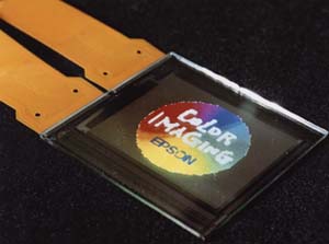
In an innovative approach to polymer display fabrication that leverages the liquid form of the materials, researchers have explored the use of ink jet printers to deposit the individual pixels of the display. Now engineers at Seiko-Epson and Cambridge Display Technologies have teamed to refine the ink-jet process (see Figure 1), demonstrating a prototype 2.5-in., full-color, video rate light-emitting polymer display.
Small molecule technology, developed first, has a substantial lead in the OLED race to market (see SID 2000: OLEDs steal the show at Society for Information Display annual meeting). Polymer manufacturers have developed a range of materials covering the full spectrum, in some cases with better fidelity to CRT display colors than small molecule materials. Until recently, however, the only way to deposit the material was by spin-coating, which essentially meant monochrome.
In a color polymer display, each pixel consists of a trio of red, green, and blue subpixels, in turn formed of three subpixels of that color—nine pixels, all told. In theory, it is feasible to spin-coat polymers onto a substrate, then pass them through a lithographic patterning and etch process to produce the requisite patterns, but practically speaking, the approach is cost and time prohibitive. "You could lithographically pattern them," conceded Cambridge Display Technology technical director Jeremy Burroughes, "but it's expensive. It takes away the advantage of wet processing." Enter Seiko-Epson, which in late 1996 teamed with Cambridge Display to develop the ink jet process.
Challenges to the process
In the ink jet process, a piezoelectric actuator squeezes a vessel of polymer to eject a droplet from a narrow nozzle onto a substrate. The Cambridge Display team used solvents doped with 1 to 2% active material by weight to transport the polymer to the substrate in 30 µm droplets. The solvent evaporates to leave a film 1000 Å thick.
Not surprisingly, the development program was not as simple as loading up cartridges of commercial polymers in a standard office ink jet unit. The team had to modify the ink jet heads to withstand solvent-based polymers, and redesign the nozzle plate so that the contact angle between the nozzle jet and the solvent would result in stable droplet formation.
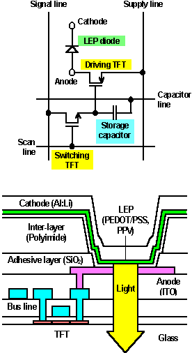
The substrate is structured to form 30 µm diameter wells (see Figure 2). In order to compensate for the droplet flight angle deviation and head placement accuracy, the surface free energy between the bottom of the well and the sidewalls was modified so that the solvent contact angle was higher for the sidewalls than the well. This results in a droplet wetting the well, even if it just clips the edge of the well.
The team also had to tune the viscosity of the solvent-borne polymer to achieve the desired 1000 Å thickness of the dried film. Interestingly, in the face of high sheer forces, the viscosity of some polymers changes, then slowly relaxes back. Success required the development of materials with constant viscosity in the face of mechanical force.
Putting the pieces together
The prototype display consists of a polysilicon back-plane incorporating an active matrix drive. Each sub-pixel is controlled by two switched thin film transistors, plus one storage capacitor. The back-plane also features integrated row and column drivers.
The design uses area division and time division to achieve 16 level gray scale imaging. Using three sub-pixels per color provides four gray levels, assuming the pixels are equal area.
To produce the display, the drive circuitry is first manufactured, then the pixel structure (indium tin oxide and cladding walls) is applied. Next, the ink jet process produces the pixel array, and finally, a global cathode—a metal layer covering all the pixels—is deposited.
For the current display, packaging is fairly rudimentary, with the group simply using an epoxy glass seal. Although much has bee made of the sensitivity of polymers to water vapor and oxygen, Cambridge Display has shown that devices stored for greater than a year show the same device characteristics as when they were made, said Burroughes. Given this data, the epoxy glass seal may well be effective for certain applications.
Performance
Though the total display size is 2.5 in., a portion of that is occupied by driver circuitry, leaving an active region of 2 in. The 200 x 150 pixel color array is capable of full video, and is intended as a cell phone display demonstrator.
The group is still gathering test data, so performance metrics are limited. At the device research level, monochrome green displays have generated in excess of 20 lm/W for display brightness between 100 and 1000 Cd/m2; Burroughes expects the similar pixel performance from the color unit soon.
"It's designed to show off the technology," said Burroughes, but notes that the demonstration has implications for the industry. "Deposition by ink jet printing would threaten other technologies which use more conventional patterning techniques," he added, noting that manufacturing costs would drop significantly. With the ink jet process, about 50% of the material involved actually becomes an active element of a display instead of the figure of approximately 1% achieved by other technologies.
The scalability of the process alone is enticing. Companies have perfected 3 in. print heads capable of operating at 180 dpi that operate at 20 in/s print speeds and are already working on wider models. The ink jet process would not limit the throughput of manufacturing facilities, which typically require one glass movement every 30 to 60 s.
Plans call for Cambridge Display to release a product based on the prototype with two years.
By Kristin Lewotsky, Editor, Photonics Online