
Huge demand for six-in LEC GaAs pushes VGF production aside

Earlier this year, Freiberger Compound Materials (Freiberg, Germany) showed very promising new results for four-in VGF (vertical gradient freeze) GaAs substrates. Already popular for optoelectronic applications, the SI (semi-insulating) GaAs crystals are well-controlled and stable enough for electronic device applications such as HEMTs and HBTs. The company says substrates with guaranteed state-of-the-art structural and electrical properties coupled with epitaxy-ready surface are now in production.
However, Harald Rudolph, Freiberger's marketing manager, cautioned that "While VGF is selling in small volume the demand for LEC (liquid-encapsulated Czochralski) materials is by far exceeding the demand for VGF. Actually, in order to satisfy unprecedented demand of our long-term customers, Freiberger is currently expanding to increase both LEC and VGF output. Freiberger's greatest activity lies with the six-in diameter GaAs substrates. While the majority of Freiberger substrates are being delivered to customers in the United States, there is an increasing demand in the Asian region, particularly from a number of Taiwanese companies."
Freiberger is a top five supplier of 100 mm and 150 mm GaAs substrates grown by LEC. LEC is presently the dominant method for the crystal growth of SI GaAs with 85% of the market, but VGF is popular amongst epitaxy customers. The SI GaAs substrate market was worth US$185 million last year and is expected to double by 2004.
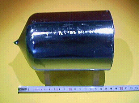
Freiberger is building a new factory emphasizing six-in SI LEC wafers. Already, it has invested $50m in "Fab 2," the first stage of a larger project with planned funding up to $155m overall, depending on market demand.
The rapid growth of epitaxy-based microelectronic devices has led to an increase in demand for low etch pit density (EPD) substrates. This type of substrate offers improved performance for some device structures. Using computer-modeling techniques, Freiberger developed a low temperature gradient VGF furnace specifically for the growth of low EPD GaAs crystals. The furnace is designed to accommodate crucibles up to 360 mm long, and with a maximum length to width ratio of two, thereby allowing growth of either 100 mm or 150 mm diameter ingots. The process has matured to the point where it has now been introduced into regular mass production.
The SI electrical properties are achieved via a multi-step post-growth annealing process developed in-house and tailored specifically for this low-EPD material. The mean dislocation density measured on 100% of the wafer area is typically below 5,000 cm-2. In the centre of the substrate, the dislocations are arranged in a cellular structure with a mean cell diameter of about 5 mm. Towards the edge of the substrate, the cellular pattern typically dissolves, resulting in weak minima of the dislocation density in <110> directions. The etch pits do not tend to accumulate in any specific location on the substrate, says Freiberger.
In order for the material to be semi-insulating (i.e. resistivity >1 x 10⁷ ohm cm), certain compensation conditions must be met. Crystals from Freiberger ´s VGF process meet these conditions throughout the entire bulk of the ingot, indicating that the residual donor concentration is sufficiently low (<2 x 1014cm-3 as measured by GDMS).
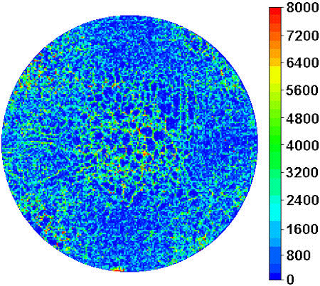
Mapping of the substrate reveals excellent uniformity of the resistivity. It indicates that both the EL2 and carbon concentration are homogeneously distributed through the material. In the topogram of the EL2 distribution - which averages about 1.2 x 1016cm-3 - variation across the substrate is typically less than 5%.
Freiberger has extensive experience in preparing epi-ready substrates for both molecular beam epitaxy (MBE) and metallorganic chemical vapor deposition (MOCVD) applications. The company manufactures three-, four-, and six-in SI GaAs substrates. It is also a producer of three-in semiconducting (SC) LEC GaAs wafers and four-in SC VGF-grown GaAs.
About the author
Roy Szweda is a freelance writer based in the United Kingdom.
For more information contact:
Harald Rudolph, Freiberger Compound Materials GmbH, Am Junger Löwe Schacht 5, D-09599 Freiberg, Germany. Tel: +49 3731 280 0; Fax: +49 3731 280106.
Donald J. Capo, Freiberger Compound Materials USA, Inc., 4259 West Swamp Road, Doylestown, PA 18901. Tel: 215-345-6445; Fax: 215-345-6298.