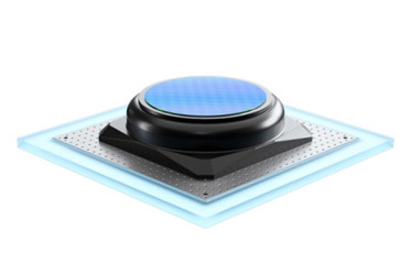
Highly-Dynamic 4-Axis Piezo Wafer Stage For Inspection And Metrology

The semiconductor industry's relentless pursuit of smaller, faster, and more efficient devices demands unparalleled precision in manufacturing processes. Wafer inspection and metrology, in particular, require motion systems capable of subnanometer accuracy to detect and analyze defects that could impact product yield. PI's latest innovation, a hybrid piezo wafer nanopositioning stage, offers a groundbreaking solution that meets these stringent requirements.
By combining the advantages of piezo technology with a unique hybrid kinematics configuration, PI's new stage delivers exceptional performance in terms of accuracy, dynamics, and crosstalk suppression. Its compact design, high integration level, and innovative control capabilities make it an ideal choice for OEMs seeking to streamline their design processes and reduce equipment complexity.
The stage's four independent degrees of freedom—tip, tilt, Z, and rotation around Z—enable precise wafer positioning and scanning. An integrated wafer lift facilitates loading and unloading, further enhancing efficiency. The hybrid kinematics configuration, featuring specialized piezo actuators, provides fast step-and-settle over long travel ranges and real-time dynamic motion over small areas.
In the following sections, we will delve deeper into the technical specifications and capabilities of PI's hybrid piezo wafer stage, highlighting its advantages over traditional electromagnetic solutions.
Get unlimited access to:
Enter your credentials below to log in. Not yet a member of Photonics Online? Subscribe today.
