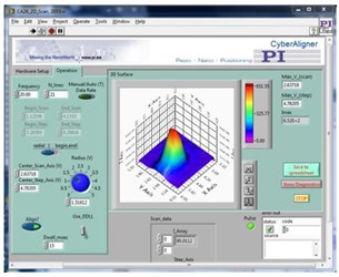
From Patterned Wafer To Packaged Device: Optical Alignment For Packaging and Test In SiP

As photonic and electronic devices began to converge, bandwidth, efficiency, and functionality improved significantly. On the flip side, testing and packaging these silicon photonic (SiP) devices has proven to be a challenge. Testing conventional microcircuits can be done through physical contact, conventional positioning control devices, and visual inspection. On the other hand, photonic devices require non-contact and nanoscale alignment between the hybrid device under test and a probe fiber or other element. And we haven’t even begun discussing the complications involved in packaging such devices.
Overcoming the testing and packaging challenges in silicon photonic devices is far from impossible though. Download the white paper to learn how a fast, multi-channel optical alignment solution can help.
Click here for a video demonstrating silicon photonics test platforms and fast multi-channel alignment engines.
Get unlimited access to:
Enter your credentials below to log in. Not yet a member of Photonics Online? Subscribe today.
