
3-DOF Precision Positioning Stages Supporting Laser Assisted Wafer Slicing

1. Laser Assisted Wafer Slicing
Staccato like flashes of blue and red intersect with an audible hiss as the lights retract tracing curvilinear arcs, illuminating the canyon of this distant lunarscape. It’s here in this fictional canyon that materials cleave along precise planes cut by coherent light sources without collateral damage. As we turn away from science fiction to science reality, the same scene is playing out in wafer fabs across the world with semiconductor materials.
As today’s technology becomes more advanced, the demand for ever decreasing sizes of features with more complex designs increases; and this means the manufacturing process of these semiconductors has to adapt. Lasers enable a wide variety of applications in semiconductor manufacturing. Major semiconductor processes, including laser cutting and slicing, integrate lasers to allow extremely high throughput with better process defect control for sustainably higher yields. Conventional techniques of slicing SiC ingots to wafers are generally performed using diamond- or slurry-based wire sawing processes. These sawing processes lead to substantial kerf-loss of precious material, which increases the cost per wafer.
Video: 5-DOF Stage for Wafer Stealth Dicing / Semiconductor Wafer Dicing
The principle of laser cutting is to use an ultra-short pulse laser to condition a defined layer within the material, creating a planar modified region weak enough to allow the entire wafer to be controllably cleaved from the ingot. Depending on the material and by optimizing the laser process parameters and beam delivery (i.e. pulse width, intensity, focused spot beam profile, etc.), the manufacturers are able to control this deformation in the material with no thermal damage to the top and bottom interface of the sliced wafer.
An external force (e.g. bonding force and pressing force) guides the cracks to precisely split the material along the laser conditioned layer.
1.1. Advantages in Comparison with Traditional Wafer Cutting Techniques
Laser modified cutting is the fast and cost-efficient solution for the ever-increasing demand and cost challenges of the semiconductor industry. This technique avoids the typical kerf-loss of wire saws in the process of slicing ingots to wafers resulting in significant yield improvement in SiC wafer production (without a need to increase crystal growth capacities). It also enables sub-100 µm thin SiC made devices.
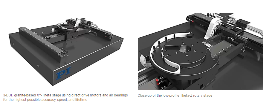
2. PI XY-Theta Stage: 3-DOF Motion System to help Laser Slicing Processes
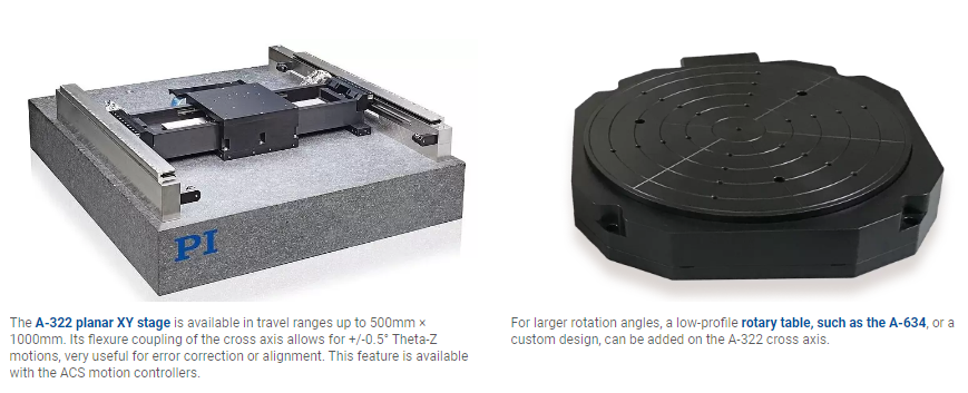
2.1. A-322 High Performance XY Planar Stages and Motion Systems
The A-322, a high performance XY planar motion system with a lapped flat granite base, provides excellent dynamics, and high guiding accuracy, making it an ideal base platform to meet the most demanding motion performance requirements of ultra-precision laser processing.
This multi-axis motion platform features 3 large ironless (zero cogging) linear motors in combination with 3 high resolution, low CTE absolute encoders (1nm resolution) with BiSS-C signal output. Running on a thin film of laminar air, it provides frictionless, smooth, highly dynamic motion throughout the process, a prerequisite for accurately following the most complex trajectories.
Video: ACS advanced 3-DOF gantry control algorithm explained with the A-322 XY-Theta stage
This 3-motor, 3-encoder gantry configuration means three linear axes are coupled to create two axes of linear motion and one axis of rotational motion (X, Y, Theta-Z). The X-Axis, Y-Axis, and Theta-Z Axis all have separate control loops for linear and rotational motion control, which results in simplified tuning, without any fighting between loops. This translates to higher throughput and performance.
The stage is designed with a flexure coupling between the X and Y axes to allow up to +/-0.5° of Theta-Z rotational motion. This Theta-Z motion is used for active yaw compensation to improve performance and simplicity of operation.
2.1.1. A-322 Product Variants
The A-322 planar XY + Theta stage product family is currently offered in three levels of performance.
A-322 XY Stage Base Model. Includes all the features described above. Uses medium-sized linear motors for moderate dynamic performance.
Acceleration: Up to 0.5g (based on payload)
A-322 XY Stage Plus Model. Enhances the base model with the use of larger linear motors with water cooling of the motors for increased speed, acceleration, and duty cycle performance. The customer must provide cooled water to the stage.
Acceleration: Up to 2.0g (based on payload)
A-322 XY Stage Ultra Model. Enhances the Plus model with the addition of a 4th motor and encoder (added to the X axis) for enhanced accuracy and repeatability suitable for large-size payloads (i.e., flat panel applications).
2.1.2. Self-locking Feature provides Higher in Position Stability
The stage can be equipped with a dynamic solenoid valve to turn the vertical lift air supply on and off for the cross-axis air bearing. By turning the lift air supply on or off while keeping all the other air supplies turned on, the stage position can be locked in place. The stage uses vacuum preload in the vertical direction, which provides the locking force via friction against the granite. This locking is done while the servo loops are enabled, which prevents parasitic motion in the X-Y directions during the transition.
2.2. A-63X High Performance Air Bearing Rotation Stage
PI low profile rotary air bearing stages (models A-634, A-635, A-638) feature a high performance 3-phase brushless direct drive torque motor for the best dynamics and motion performance. They offer excellent positioning accuracy using high resolution, direct-measuring absolute and incremental encoders. The rotary tables are designed to offer excellent stiffness and high load capacity while they are compact with low overall mass. The tabletop is precision-ground flat to minimize distortion and the motion platform is manufactured to support 200mm, 300mm, and 450mm wafers and panels.
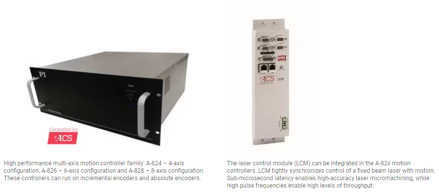
2.3. ACS Based Motion Controller with State-of-the-Art Features
A-8XX ACS based multi-axis motion controllers offer advanced multi-axis motion profiling algorithms to build complex optimized trajectory paths. These trajectory paths are precisely followed with tight servo loops using real time disturbance attenuation enabling world leading process results.
Employing Laser Control Modules (LCM) and Laser Control Interfaces (LCI), ACS motion control solutions enable high-speed, tightly synchronized laser triggering to empower high-accuracy laser micromachining.
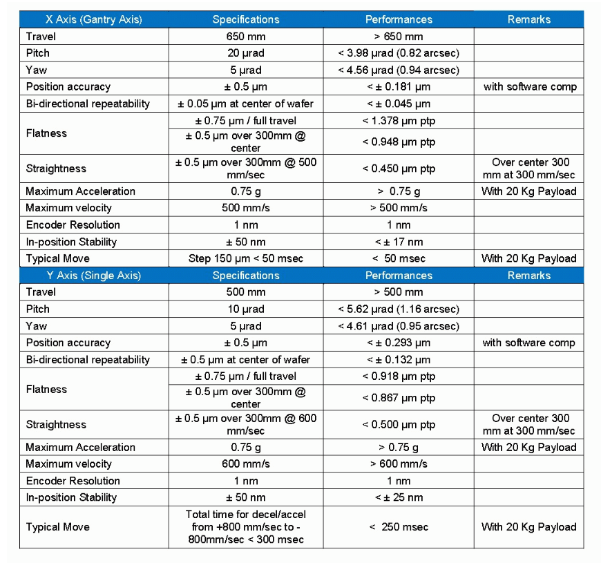
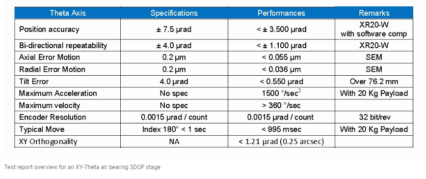
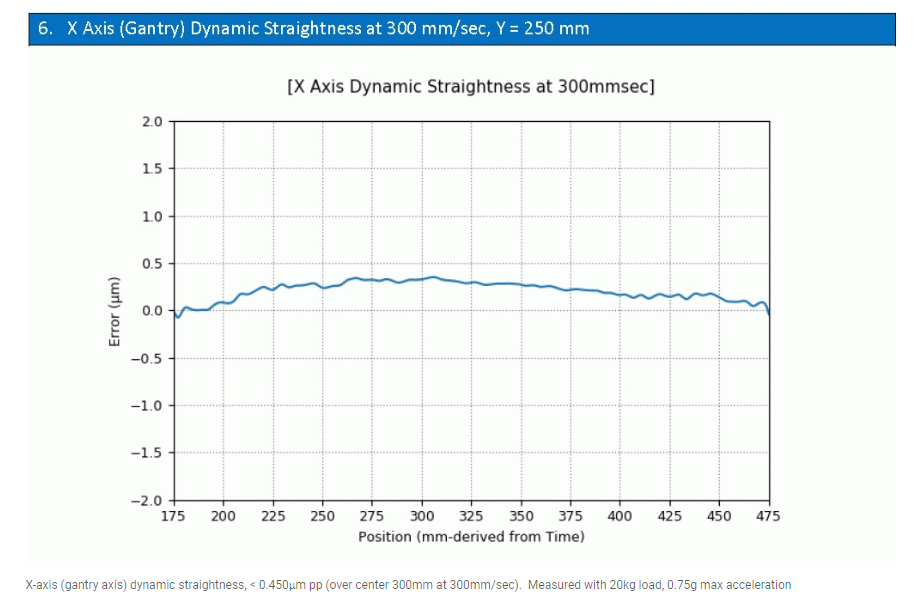
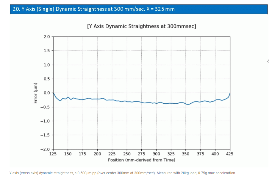
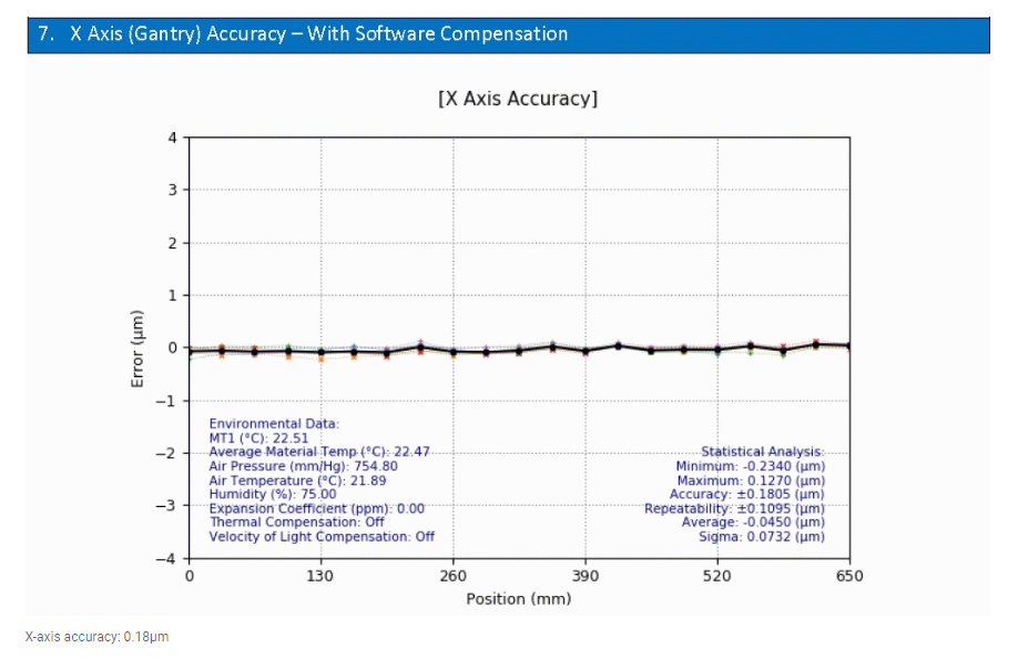
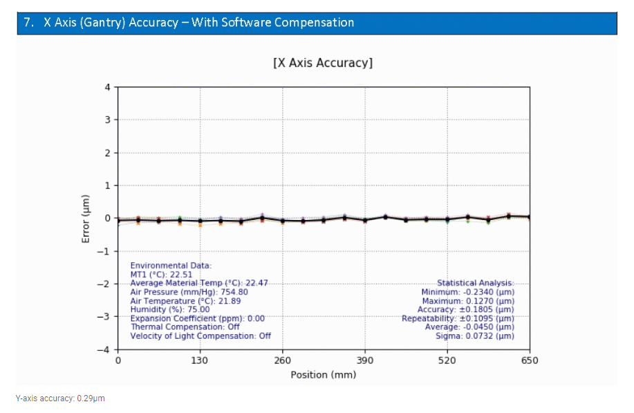
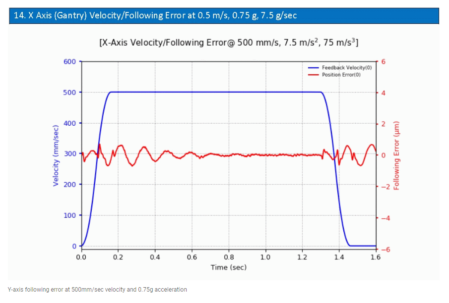
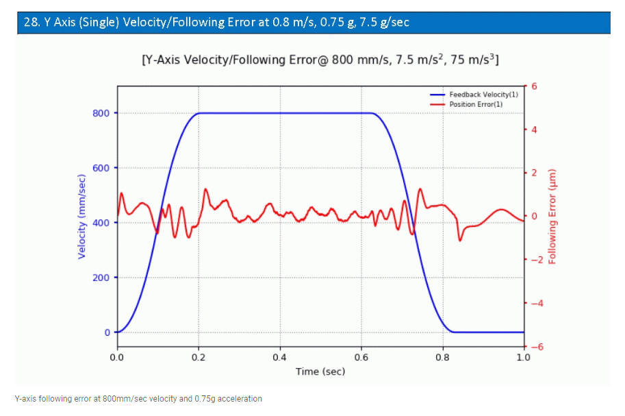
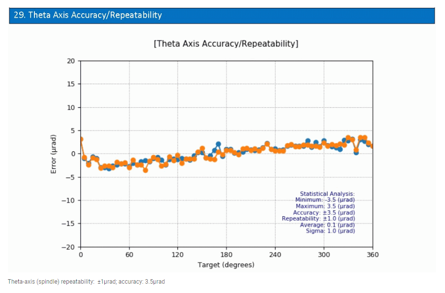
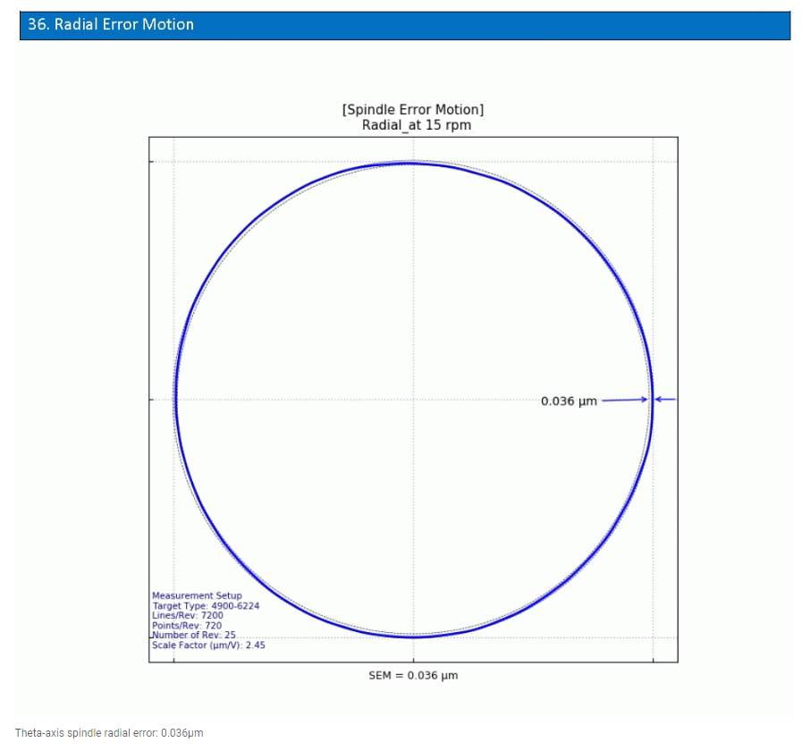
Test Data of an XY-Theta Air Bearing Stage
The following data and graphs are a selection of the tests PI runs during the qualification process of a multi-axis air bearing stage. Additional information is available on request.
Multi-Axis Nanopositioning Stages for the Semiconductor Industry - Get Support from A PI Engineer
If you would like to learn more on high performance motion systems for semiconductor manufacturing, test and metrology, test and other multi-axis motion and positioning assemblies, please do not hesitate to contact our engineers directly.