
Direct electrical pumping powers 1.3 µm VCSEL

By: Yvonne Carts-Powell
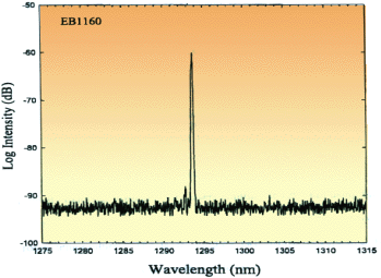
Vertical-cavity surface-emitting lasers (VCSELs) rule the 850-nm data communications market because they are cheaper to make and more energy efficient than edge-emitting semiconductor lasers. For the longer-distance and higher-data-rate telecommunications world, however, users need longer wavelengths of 1.3 and 1.55 µm, at which there is less attenuation in the optical fiber. Thus far, VCSELs have been limited in this market because no one had developed a direct electrical pumping scheme. Market deployment just took a giant leap closer as researchers at Cielo Communications (Broomfield, CO) and Sandia National Laboratories (Albuquerque, NM) developed an electrically pumped VCSEL that emits at 1.3 µm (see Figure 1).
One-step growth, one-step pumping
Two years ago, researchers at W.L. Gore (Newark, Delaware) announced a 1.3 µm VCSEL, but it was optically pumped by a 850-nm VCSEL wafer bonded to combine the mirrors and active regions of the two devices into a single unit. Wafer bonding adds a tricky step to the fabrication process, raising questions about the feasibility of volume production.
Developed in a Cooperative Research and Development Agreement (CRADA) between Cielo and Sandia, the new 1.3 µm device operates with direct electrical pumping and can be grown in a single process—without requiring wafer bonding.
The active region of the device is grown from indium gallium arsenide nitride (InGaAsN), with gallium arsenide (GaAs) mirrors. The material was initially developed by Hitachi of Japan in the mid 1990s. "The key to making this work was to optimize the material quality of the InGaAsN and to make subtle changes to the rest of the structure," says John Klem at Sandia. "The device is grown in a single epitaxial growth run," he adds. "We believe that eliminating the wafer bonding results in a much more manufacturable process."
Klem says, "We're also doing it all on a GaAs substrate, and with AlGaAs/GaAs DBRs [distributed Bragg reflectors], which means that all of the processes which have been developed over the years for short wavelength VCSELs can be used."
Markets
In addition to the telecom market, this VCSEL also can allow the datacom market to move to the longer wavelength. This would allow data transmitting system to leverage the huge investment that has been made in developing 1.3 µ systems for the telecommunications world. In his plenary address at the Conference on Lasers and Electro-Optics (CLEO 2000; San Francisco; May 7-12), Steve Joiner of Agilent Technologies identified long wavelength (1.3 µm) VCSELS as being a key element in propagating VCSELs into the data network. "We'd prefer that the 850 nm components be gone," he said. "We need 300 m distance at high speed, with minimal physical interface [between datacom and public network]."
The VCSEL's lifetime is unknown at this point, although Bob Mayer of Cielo comments that the device has been shown to operate at temperatures up to 55° C. The next steps are to perform reliability testing and bandwidth characterization. Because Cielo sells communications components, rather than the lasers themselves, the company is also working on building the VCSELs into products. "We expect to have them on the market within 12 months," says Mayer.
About the author…
Yvonne Carts-Powell is a freelance science and technology writer based in Massachusetts.