'Black Holes' In Silicon Enable High-Speed Photodetector
By Jof Enriquez,
Follow me on Twitter @jofenriq

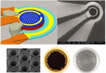
Electrical engineers at University of California, Davis, and Silicon Valley startup W&WSens Devices have developed a new type of photodetector that relies on tiny, tapered "black holes" on a silicon wafer to trap light. Such a high-speed, high-efficiency photodetector can better handle the growing volumes of data traffic and higher bandwidths in data centers today.
Silicon can act as a photodetector to convert pulses of light into electronic pulses. However, a dilemma for engineers is that a thin piece of silicon works quicker but loses many photons, and making it thicker allows it to capture most incoming photons to generate a flow of electrons, but slows down the process. As a result, some engineers have experimented with alternative materials like graphene, indium phosphide, and gallium arsenide, which is up to ten times more efficient than silicon.
Yet today, silicon still holds a commercial advantage over the more expensive gallium arsenide — which is used in niche devices, justifying their higher cost, but is challenging to monolithically integrate with silicon electronics. In order to reduce cost and drive performance, researchers at UC Davis are thinking of ways to maximize the utility of silicon.
“We’re trying to take advantage of silicon for something silicon cannot usually do,” said Saif Islam, professor of electrical and computer engineering at UC Davis, who co-led the research, in a news release. “If we don’t need to add nonsilicon components and can monolithically integrate with electronics into a single silicon chip, the receivers become much cheaper.”
The team experimented with adding several tiny holes, tapered toward the bottom, to a two-micron thick silicon wafer. The microstructure works by letting photons enter the holes and get pulled sideways into the silicon, making them travel through between 30 and 40 microns of silicon like ripples of waves on a pond.
“We came up with a technology that bends the incoming light laterally through thin silicon,” said Islam, whose team built an experimental photodetector and solar cell using the new technology.
In an article published online April 3 in the journal Nature Photonics, the engineering team wrote that its demonstration achieved "an ultrafast impulse response (full-width at half-maximum) of 30 ps and a high efficiency of more than 50%, for use in data-centre optical communications. The photodiode uses micro- and nanostructured holes to enhance, by an order of magnitude, the absorption efficiency of a thin intrinsic layer of less than 2 µm thickness and is designed for a data rate of 20 gigabits per second or higher at a wavelength of 850 nm. Further optimization can improve the efficiency to more than 70%."
This research project was supported by the S.P. Wang and S.Y. Wang Partnership, the U.S. National Science Foundation, and the Army Research Office.
