A Breakthrough In Silicon Photonic Research

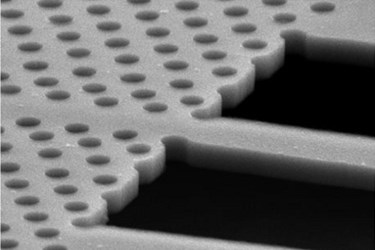
An international group of researchers recently completed the first experimental demonstration of a soliton-effect pulse compression in a silicon photonic crystal. The findings could be a significant step toward the development of photonic chips at the micron scale.
Andrea Blanco-Redondo and Dr. Chad Husko of the University of Sydney’s CUDOS (Australian Research Council Centre of Excellence for Ultrahigh bandwidth Devices for Optical Systems) led the project, which also included members from the University of St Andrews (Scotland) the University of York (England), and Sun Yatsen University (Guangzhou, China).
Historically, examining optical soliton waves within silicon has been difficult due to the presence of two photon absorption and accompanying free carriers, which disrupt the “the canonical dynamics of optical solitons,” according to the group’s paper in the journal Nature Communications. Despite the interference, the researchers were able to compress 3.7 ps pulses to 1.6 ps using less than 10 pJ of energy.
For the experiment, the researchers used “a dispersion-engineered slow-light photonic crystal waveguide” in conjunction with “an ultrasensitive frequency-resolved electrical gating technique” in order to “detect the ultralow energies in the nanostructured device.” Their measurements were confirmed by a nonlinear Schrödinger model. The researchers also noted that, “using picosecond input pulses [were] critical to these observations.”
The demonstration could be significant for the development of optical circuits using materials with CMOS compatibility, like silicon, for on-chip communications. In a news story on the University of Sydney website, Husko said that, “Optical soliton waves in a silicon photonic crystal chip the size of a human hair could add key insights to future integrated optical communications systems.”
The experiment is perfectly aligned with the overall mission of CUDOS, which is to develop the world’s best photonic chips by making them smaller, faster, and greener.
Understanding solitons within silicon is especially pertinent to the development of smaller photonic chips. Soliton propagation in silicon functions at the micron scale, which is roughly the size of a human hair. The use of silicon could enable the development of miniaturized optical components with soliton-based functionality for photonic chips.
Professor Ben Eggleton, CUDOS director and co-author of the research, acknowledged the significance of these findings when he said, “this latest breakthrough … is of both fundamental and technological importance.”
Image Credit: Nature Communications 5, Article number: 3160 doi:10.1038/ncomms4160
