
Understanding Diamond And Its Relationship With Optics
By Henk De Wit, Element Six

Diamond is known across the world as the ultimate luxury, often in relation to jewellery. However, diamond’s extreme physical properties make it particularly useful for a diverse range of industrial uses.
The unique mechanical, optical, thermal, and electrochemical properties possessed by diamond facilitate its application in extremely challenging environments, and it has proven to be a successful material in the world of engineering.
Diamond’s unique physical properties are a direct result of its crystalline structure. The carbon atoms are arranged in a very tight packing through four strong tetrahedral covalent bonds. This results in a very dense and rigid crystal structure.
Natural Or Synthetic?
Both natural and synthetic diamonds have the same crystal structure, leading to the same set of physical properties. Synthetic diamonds, however, offer the possibility of control over defects during synthesis, accomplished through precise control of the process parameters. In this way, manufacturers can tailor the synthetic diamond’s properties for optimum use in a wide range of applications.
Two Production Methods
There are two different production methods for synthetic diamond. One widely used method is to mimic the process of how natural diamond is created in the earth’s crust, using simultaneously high pressure and high temperature, also known as the HPHT method. The conditions under which diamond forms are generated within custom-designed presses weighing hundreds of tons. A way to visualize these conditions is having the Eiffel tower upside down on top of a cola can at a temperature of 1500°C.
The other method is chemical vapor deposition (CVD). This method works at lower temperatures and pressures. A plasma containing carbon and hydrogen atoms is created by heating a gas mixture, comprising methane (CH4) or carbon dioxide (CO2), along with hydrogen gas.
The gas mixture is heated, using microwaves, to transform the gas mixture into a plasma, reaching temperatures ranging between 550°C and 1200°C. Under the correct levels of pressure and temperature, carbon atoms are deposited on a suitable substrate, which step-by-step creates the carbon lattice. Typical growth rates are expressed in µm/hour.
By using high-purity gasses and ruggedly constructed reactors, the chemical impurity level can be controlled to parts per billion (ppb) level. Through this method, the diamond’s properties can be carefully manipulated.
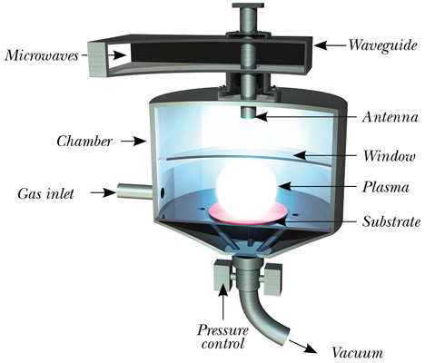
Fig 1 — Typical microwave plasma-assisted CVD diamond reactor.
By controlling growth rates and impurity levels, the CVD method lends itself to the manufacture of both high quality, free-standing single crystal and wafer-scale, poly-crystalline synthetic diamond.
Boron-doped CVD diamond (BDD) provides a clear demonstration of how diamond properties can be manipulated. By adding diborane (B2H6) to the gas mixture and heating the plasma to over 2000°C, boron is incorporated in the diamond lattice, transforming it from an electrical insulator into an electrical conductor. BDD wafers of up to 150 mm diameter and 1 mm thickness can be produced in this way. This process ensures the material is the ideal base for electrodes to be used in electrochemistry and chemical sensing.
Another example relevant to the optical realm aims to keep the diamond’s intrinsic and extrinsic defects to a ppb level, creating a very pure single crystal material featuring ultra-low birefringence and low absorption properties — necessary for intra-cavity use of diamond optics in high-power solid-state lasers.
How Can Diamond Be Shaped?
Synthesizing CVD diamond is only half of the story. To create the products required for various applications, the raw diamond must be transformed into differently shaped products — including ATR prisms, hemispherical lenses, output couplers, or exit windows, to name a few. Special engineering technology has been developed to manufacture such products (Fig. 2).
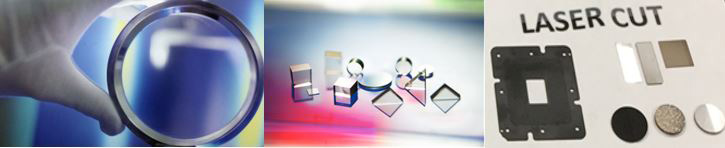
Fig. 2 — (L-R) Examples of lapped, polished, and laser cut diamond wafers and samples.
Specifications for surface quality of poly-crystalline CVD achieved by processing are:
- Lateral dimensional tolerance = -0.0/+0.1mm
- Thickness tolerance = ±0.050 mm
- Polished Surfaces: Ra < 5 nm (Nucleation side over 25mm)
- No more than ± 10 nm variation of Ra (over 50 mm diameter)
- Flatness < λ/30 @ 632nm (over 35 mm diameter)
New processing technologies include focused Ion beam surface treatment, laser-induced thermal ablation, and laser-assisted chemical etching in oxidative environments. Diamond shaping, in all cases, starts with a graphitization step, which can be accomplished through any of the above methods. Once this takes place, this graphite layer is oxidized to form carbon dioxide. As a result, diamond polishing has carbon dioxide as its primary form of debris.
Diamond’s Applications in Optics
Being the hardest material known, diamond can be used in a variety of abrasive applications. Diamond-based tooling allows special composite materials used in automotive and aerospace applications to be machined where conventional tooling fails to do so.
The combination of diamond’s broadband transparency, chemical inertness, low absorption, and highest-known thermal conductivity offers benefits for applications running at either high power levels or high-power densities; poly-crystalline CVD diamond optical components in high-power lasers and CVD diamond heat-spreaders in high-power RF-electronic devices are prominent examples. In all cases, the diamond enables the application to run at considerably higher performance levels compared to designs based on conventional materials.
An example of CVD diamond’s capabilities being utilized is the multi-national project Fusion for Energy (F4E), also known as the ITER project. The F4E project is building a reactor for nuclear fusion in Cadarache, France, with the aim of producing 50 megawatts of electrical power as a new, sustainable source of energy. This reactor mimics the process of the sun, where hydrogen fuses to form Helium with the release of huge amounts of energy.
In the reactor, a plasma is heated to fusion temperatures using high-power mmWave radiation, generated by so-called gyrotrons. Each gyrotron generates 1 megawatt of radiation, transmitted through an output window. CVD diamond is the only material that can handle this level of power without being destroyed under operation, due to diamond’s low absorption of millimeter radiation, along with its superb heat transfer properties. These diamond windows will also enable the next generation of gyrotrons, capable of handling even 2 megawatts.
Another popular application of optical single-crystal diamond is attenuated total reflectance (ATR) spectroscopy. In this spectroscopic technique, a prism is brought into contact with the sample to be measured, and a broadband source is propagated through the prism by total internal reflectance. Diamond’s low loss and broadband transmission are ideal optical properties for this application. In addition, the strength and hardness of diamond make the prisms much more durable than prisms made of other materials.
When measuring diamond’s other properties, it is important to note the most extreme application currently known for CO2 lasers — extreme ultraviolet lithography (EUVL), where the ultimate stability of diamond optics is not determined by the diamond substrate, but rather by the thin-film AR coating.
Summary
While most people think of diamond as a precious gemstone, known for its optical brilliance and its hardness, synthetic diamond delivers benefits for a diverse range of industries, including for many optical applications.
When compared to natural diamonds, laboratory synthesis of diamond provides control over defects typically found in natural diamond, ensuring a higher and more consistent performance throughout.
About The Author
Henk de Wit has served as CVD diamond optics business manager at Element Six since joining the company in 2007. His primary focus within the business centres on the development of new solutions for existing markets and identification of new application areas. Before joining Element Six, he held a variety of roles and assignments during his 22 years at Royal Philips Electronics. His assignments with Element Six span a range of roles in R&D, with a particular focus on electronic components, ceramics, imaging devices and optical storage. Henk holds a MS in Chemistry and a PhD in Mathematics and Science.