South Koreans Develop World's Thinnest Photodetector
By Jof Enriquez,
Follow me on Twitter @jofenriq

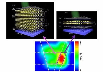
South Korean scientists unveiled what they claim to be the world's thinnest photodetector, consisting of a 1.3 nm layer of molybdenum disulfide (MoS2), sandwiched between graphene layers and mounted over a silicon base. That's about ten times smaller than standard silicon photodiodes, a feat that could open up a new dimension in the design of future electronic and optoelectronic devices.
In order to extend the usability of graphene as a material for such devices, scientists at the Center for Integrated Nanostructure Physics, within the Institute for Basic Science (IBS) in Daejeon, South Korea, built a single-layer graphene/ MoS2/graphene heterostructure to observe how efficient it can get in converting light and generating an electric current.
"A device with one layer of MoS2 is too thin to generate a conventional p-n junction, where positive (p) charges and negative (n) charges are separated and can create an internal electric field. However, when we shine light on it, we observed high photocurrent. It was surprising! Since it cannot be a classical p-n junction, we thought to investigate it further," said Yu Woo Jong, first author of this study, in a news release.
The scientists then built and compared two devices: one with the monolayer of MoS2 between two graphene sheets, and another with seven layers of MoS2 stacked between graphene sheets, mounted atop a silicon base. The single-layer device absorbed less light, as expected. But it did show higher photoresponsivity than the multi-layered device.
"Usually the photocurrent is proportional to the photoabsorbance, that is, if the device absorbs more light, it should generate more electricity, but in this case, even if the one-layer MoS2 device has smaller absorbance than the seven-layer MoS2, it produces seven times more photocurrent," added Yu.
As light hits the single-layer device, photo-excited electrons from the MoS2 layer encounter a higher energy barrier produced by the silicon dioxide layer below, so it tends to tunnel from the MoS2 layer upwards to the top graphene (GrT) layer – where the air on top has reduced the energy barrier – to produce an electric current.
This movement of photo-excited electrons in graphene layers is analogous to a group of people deciding which mountain to climb to get out of a valley.
In the one-layer device, "one mountain is taller than the other, so the majority of the group choose to cross the smaller mountain. But because we are considering quantum physics instead of classical electromagnetism, they do not need to climb the mountain until they reach the top as they can pass through a tunnel. Here, the idea is that electric current is generated by the flow of electrons, and the thinner device can generate more current because more electrons flow towards the same direction,” stated the researchers.
In contrast, in the multi-layer MoS2 device, the energy barriers between the top graphene and bottom graphene are symmetric, therefore the electrons have the same probability to go either side (an equal number of people would climb opposite mountains), and thus reduce the overall generated current. Both electrons (negatively-charged) and holes (positively-charged) also tended to move too slowly through the junctions between graphene and multiple layers of MoS2, leading to their undesired recombination within the MoS2 layer.
"Spectral-dependent studies further show that the internal quantum efficiency in one-layer MoS2 can reach a maximum of 65%, far higher than the 7% in seven-layer MoS2. Our theoretical modelling shows that asymmetric potential barriers in the top and bottom interfaces of the graphene/one-layer MoS2/graphene heterojunction enable asymmetric carrier tunnelling, to generate usually high photoresponsivity in one-layer MoS2 device," the scientists wrote in their study, published in Nature Communications.
"This device is transparent, flexible and requires less power than the current 3D silicon semiconductors. If future research is successful, it will accelerate the development of 2D photoelectric devices," said Yu.
Other developers of graphene photodetectors are stacking other novel two-dimensional (2D) materials to take advantage of graphene’s optical properties such as broadband absorption, ultrafast response and gate tunability. Recently, another group of European researchers have built a quantum LED using layers of graphene and transition metal dichalcogenides (TMDs).
