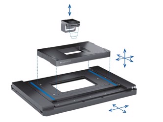
Piezoelectric Positioning Equipment For Nanoscale Microscopy & Imaging

Conventional optical microscopy is limited to a sample magnification of approximately 1000x, due to the wavelength range of visible light (400—700nm). Two distinct points on a sample can be optically resolved using a standard microscope if they are no closer than ~0.2 micrometers (μm) to one another.
Although groundbreaking in its time, the compound microscope has quickly fallen behind alternative tools capable of performing high-precision materials characterization or insights into molecular activities on the nanoscale.
Numerous techniques have been developed to overcome the limited resolving power of conventional microscopes. Super-resolution optical microscopy, scanning electron microscopy (SEM), atomic force microscopy (AFM), and much more have emerged as suitable candidates for surface metrology. All of these methods require some kind of motion – in the case of SEM, an electronic beam can be deflected without using mechanical components. In the case of AFM and super resolution optical microscopy, precision mechanisms are required to move the probe or sample.
Get unlimited access to:
Enter your credentials below to log in. Not yet a member of Photonics Online? Subscribe today.
