
The Future Of Metasurface Optics — A Q&A With Metalenz CEO Robert Devlin

By Abby Proch, former editor

The ask from customers is usually this: Make it smaller, faster, lighter, and cheaper.
It’s true of most industries, and it’s especially true with photonics and optics. As our explorations delve deeper into space and shrink so small as to fit in places the eye can hardly see, so the technologies must also evolve.
Recently, much ado has been made about metasurface lenses. They’re incredibly compact and are increasingly producing high-quality images. What’s more, they can be made alongside semiconductors on-site in the very same foundries.
That’s what Metalenz has hooked onto. They’ve established a partnership with STMicroelectronics to streamline their supply chain and, for the first time, bring metasurface optics into consumer products on a large scale .
I recently chatted with Metalenz CEO Robert Devlin, who cofounded the company alongside Harvard University Professor of Applied Physics Federico Capasso, about the company’s beginnings, how its business partnership evolved, the challenges of integrating into consumer products, and what he believes is the future of metasurface optics.
This conversation was edited for length and clarity.
Tell me about how the group that you spun out of and how you ended up where you are today.
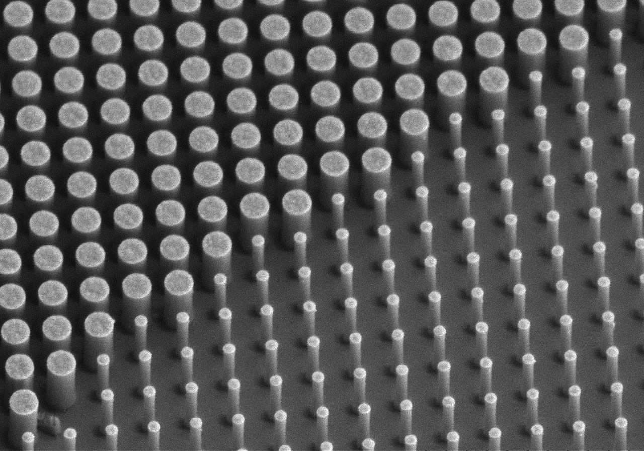
The idea with metasurface optics is to have complete control, but do it using standard semiconductor processing. All of the semiconductor fabs are working in the planar dimension. It's just layer built upon layer, only changing two dimensional layers. In 2011, our group at Harvard published a paper in “Science” that got tons of attention, tons of excitement, because lenses can now be completely flat. But while the initial proof of concept was really compelling, it was still not quite where it needed to be in terms of overall efficiency and performance.
In 2016, the year we ended up spinning the company out of the group, we showed for the first time really high-quality images that were taken with metasurfaces. And then that ended up resulting in another paper on the cover of “Science” because everyone had seen the promise of the technology. The coverage had investors in some of the largest cellphone companies in the world cold calling [Harvard School of Engineering professor] Federico Capasso. And that was a time where we were like, “OK, this is probably worth making into something real now” and decided to spin out Metalenz.
What were the challenges you faced when trying to bring metasurface optics into consumer devices?
Anyone can move the incumbent along 5% and keep their job. But if you end up taking a risk on a new technology, it's great if it works out. But if it doesn't work out, it's a big risk for these companies, especially the cell phone manufacturers where a bad lens is just a huge liability for them. And it's a huge liability for us as a smaller company to start out.
So it's really getting the customers to not just buy in to what we could do for their modules and how we could improve them, it was getting them to buy into the fact that this was going to be delivered at scale.
There's a whole host of standards to meet before you even get close to a cell phone. STMicroelectronics is a known supplier to all of these cell phone OEMs, so they already have that initial credibility. And they make their own modules and do all of that optics validation necessary for consumer electronics.
We all knew that it was going to work, but they had to show it in order to get the rest of the cell phone OEMs on board. It’s really about having confidence that it's going to last, that it's going to be reliable. STMicroelectronics just gave that credibility and experience and allowed us to really prove that out.
Was there anything that you didn't anticipate along the way that surprised you?
When getting into startups, it's often just as much about timing as it is about having a great idea. And one of the things that was a really great surprise was the year we launched was the first year that Apple's Face ID came out. The iPhone 10 launched and that was the first mass market, 3D sensing application. And that actually caused a huge growth in 3D sensing, because ultimately, all of the other OEMs in the cell phone world sit and watch what Apple is going to do and then try to replicate it.
When we were starting to look for applications, all of a sudden there emerged this really rapidly growing consumer market for 3D sensing. And since then, essentially, it's panned out for us and that market continues to grow.
I think the other piece is just the amount of convincing that needs to go in on the manufacturing side with the OEMs and the module integrators — especially for consumer devices. If you haven't shown it in manufacturing, if you haven't proven out all these things, then it's too big of a risk for them.
How did the relationship with STMicroelectronics happen, and how did it evolve?
Initially, we reached out to STMicroelectronics because the first market that made sense was 3D sensing. This was a market where the optical modules are really complex. And that's one of the biggest benefits that metasurfaces bring to optics beyond being able to move into the semiconductor foundry. It lets you reduce the complexity of an optical module by a factor of four or five.
And as we looked at who were the real leaders both from the cell phone world but also from the supplier world, the module makers, and the general solution providers, we came across STMicroelectronics.
As we started engaging with them a little bit more, it became not only clear that we could help them address their pain points they had in their module. What else became really clear was they were looking at ways to use their existing foundries. So that started the second conversation, which was, let's bring up the process to make Metalenz metasurfaces in our fabs.
How did you know that STMicroelectronics was the best fit for a partner?
It ended up being the best fit because they have both of these pieces of understanding: optics and the semiconductor fabrication. Because STMicroelectronics was already making these modules, and they were purchasing optics separately, they really understood both the optics part and the semiconductor fab part. And that's sort of a unique intersection that you don't necessarily find.
Can you tell me more about what specific consumer devices these will be in or that they are in?
STMicroelectronics has sold something like 1.7 billion of these modules to date across 200 different cell models. It's really in all of these different consumer products, laptops, cell phones, smart devices, anywhere that you really want to be able to get a 3D image to detect whether someone is in front of the computer or not.
Do you see metasurface optics and traditional optics coexisting, complementing, or replacing one another?
There’s going to be a shift in many applications for metasurfaces. But ultimately, traditional optics have been around for hundreds and thousands of years. And there will always be some use case. With something like your DSLR camera, or an industrial camera, or where form factor and price are not really key driving points, traditional optics will continue to have a place.
And in fact, there's use cases where including both a traditional optic and a metasurface optic can even give you some potential benefits. In the foreseeable future, there will certainly be a coexistence. But because of how much they simplify the system, metasurface optics will be taking more and more of the market share.
Because there are some different avenues for metasurfaces, what is the one that most excites you?
If you look at the sensing that is done on smartphones today from the optical modules, you have a visible camera and you have a 3D sensor. Technically, those are both things that human vision already do. But there’s this idea of bringing a whole new information set that we can't necessarily see with our eyes. That's just super exciting to me: What are the applications that emerge that we're not even thinking of yet once you have this in millions or billions of people's pockets?
Metasurfaces allow you to do complex forms of sensing that may have been too expensive to really proliferate broadly. Beyond just intensity and wavelength, light also has polarization information with it. And that polarization information can be used for a host of different applications, which haven't been accessible or haven't been available to consumers and end user devices.
For example, polarization can be used to tell whether a growth on skin is cancerous. You can quickly take a shot at your arm with one of these polarization cameras and send it off to a doctor rather than having to go through complex tests. Medical services are going to provide access to new information that it hasn't been able to scale because of form factor and price point constraints of complicated optical modules.
Do you have a pulse on how many other companies are producing metasurface optics, and how do you differentiate yourself from them?
We have first-mover advantage; we've been around since 2016. And our entire focus has been on metasurfaces. We also have the IP from the group where these were invented. And, we focused for the past five years on building up our own internal expertise and design tools that really help to keep us ahead.
It's also that last piece, which I mentioned, that it was initially a surprise for me how long it would take to convince people on the manufacturing side that the disk would actually not fall apart or disintegrate when they put it into their devices. Because we've been the ones that have now proven that out, it gives all of our customers the confidence that we can deliver on that.