Israeli Researchers Successfully Hide Optical Chip Under ‘Cloak Of Invisibility'
By Jof Enriquez,
Follow me on Twitter @jofenriq

Scientists at Ben-Gurion University of the Negev (BGU) are proposing a new method to obscure an optical chip by bending light around the object. This could be achieved by manipulating waves in the near field region (such as surface plasmons) of a metamaterial surface (a metasurface) on an integrated photonic structure.
Metamaterials can control the way in which light interacts with them, such that when light reflected by a metamaterial is refracted in the ‘wrong’ way, they can render objects invisible.
One approach to realizing “invisibility cloaks” is through transformation optics, whereby, instead of physically transforming the medium, its parameters are modified, so that it transforms the coordinates of the electromagnetic fields, resulting in a concealed object.
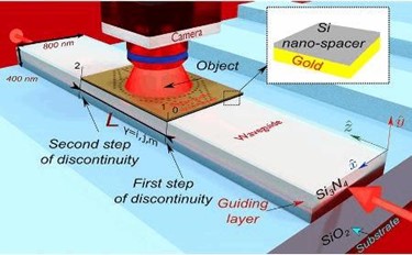
BGU researchers tested their invisibility cloaking scheme using a new, composite plasmonic waveguide with a silicon nano-spacer. The designed metasurface in the middle of the waveguide successfully deflects the evanescent waves off the object, effectively concealing it.
"Cloaking was demonstrated for a cylindrical object with diameter of 70% from the waveguide width on a high index ridge waveguide structure with silicon nitride guiding layer on silica substrate," the researchers write in Scientific Reports.
“We showed that it is possible to bend the light around an object located on the cloak on an optical chip. The light does not interact with the object, thus resulting in the object’s invisibility,” says Dr. Alina Karabchevsky, head of BGU's Light-on-a-Chip Group, and a member of the BGU Unit of Electro-Optical Engineering and the Ilse Katz Institute for Nanoscale Science and Technology.
BGU’s proposed device should have the ability to direct the flow of light smoothly around the cloaked region, such as around an optical chip, and is effective for a wide range of refractive indices and materials.
The research team is developing a prototype, but when it becomes an operational cloaking chip, it can be an extension of basic technologies, such as radar-absorbing dark paint used on stealth aircraft, local optical camouflage, and surface cooling to minimize electromagnetic infrared emissions or electromagnetic wave scattering, reports The Jerusalem Post.
"These results open the door to new integrated photonic devices, harnessing electromagnetic fields of light at nanoscale for a variety of applications from on-chip optical devices to all-optical processing," says Karabchevsky.
While BGU’s approach to build an invisibility cloak is by guiding light waves around an object, other researchers are pursuing the same goal using spatial light modulators, irradiating materials with their own specific pattern to induce transparency, or by fabricating objects that emit light themselves.
