Designing Low-Power, High-Speed Opto-Electronic Circuits For Short-Link Communication

By imec
The Need For High-Speed Electronic Circuits
Today’s information and communication technology (ICT) infrastructure, including the growing amount of data centers, requires an increasing amount of energy and bandwidth. To enable such high-bandwidth, energy-efficient data communication, optical data transmission will be key. Fiber-optic solutions are already well-established in long-reach core, metro, and access networks. Recently, they are emerging in shorter-reach applications as well, such as short-reach, inter-datacenter point-to-point links. In addition to advanced optical components, high-speed electronic circuits will remain crucial to the success of these fiber-optic solutions. They not only generate, process, and store huge amounts of data, but also interface between two very different worlds: the purely digital CMOS and the rather analog photonic devices. For example, optical data transceivers combine high-speed electronic circuits and photonic circuits. At the transceiver side, electronic drivers convert a standard CMOS bit state into an electrical signal that is compatible with the optical device. At the receiver (Rx) side, electronic transimpedance amplifiers (or TIAs) convert the photo-current (coming from e.g. a photodiode) into a standard CMOS bit state. In these opto-electronic devices, several driver and TIA circuits must be integrated onto a single chip in order to increase the system’s capacity. And this poses several design challenges. Moreover, the chip must be designed to allow the best cost-performance-power trade-off.
New High-Speed Electronic ICs For 100 Gbit/s Optical Links
For this purpose, imec and Intec_design have developed multi-channel 25 Gbit/s low-power driver and transimpedance amplifier integrated circuits (ICs), integrated into arrays. The two-channel 25 Gbit/s driver array is the fastest modulator driver and consumes only 652 mW per channel at a typical operating condition (i.e. a differential output swing of 6Vpp). The 4 by 25 Gbit/s Rx array shows a good sensitivity of -10.3 dBm at 25 Gbit/s and a power consumption of only 77 mW per channel. Both ICs were developed in a 130nm SiGe BiCMOS process. Using a SiGe BiCMOS technology is advantageous because it offers an improved overall performance at high operating frequencies.
The High-Speed, Low-Power Driver Array
For cost-sensitive, high-bandwidth applications, low-complexity signal modulation and multiplexing are preferred over coherent transmission and digital signal processing. In particular, optical duobinary modulation is a format that is gaining interest in today’s optical data transmission. Within the driver IC, the incoming data signal (a non-return-to zero signal) is first converted on chip into a duobinary signal, by using an encoder and pre-coder. A pre-driver block amplifies the input signal and drives the input of the actual driver. The data output of the driver array is subsequently fed into two separate electroabsorption modulators (or EAMs). To reduce the power consumption, different supply voltages have been used for the pre-encoder, the pre-driver, and the actual driver.

Two-channel 25 Gbit/s duobinary driver electrical test board and die micrograph
To quantify the driver’s operation, duobinary eye diagrams — a useful tool for measuring the signal quality —were taken at data rates of 28 Gbit/s. The measurements reveal an energy-per-bit performance of 23.3 pJ/bit at 6Vpp, a number that remains well below the state-of-the-art. To our knowledge, this is the fastest modulator driver with on-chip duobinary coding reported so far. Finally, two 25 Gbit/s driver arrays can be combined to realize a throughput of 100 Gbit/s.

Eye diagrams for differential drive voltages from 3 Vpp up to 6Vpp
The Compact, Low-Power Transimpedance Amplifier
The 4-channel Rx array has been designed for optical duobinary reception. An important feature of our Rx is its tight integration, resulting in a footprint that is much smaller compared to state-of-the-art solutions. Such a size reduction is important, since photonic components like photodiodes are often small compared to electronic ICs. For example, the channel pitch of our Rx is only 250 µm, which is equal to the pitch of the photodiode array.

Micrograph of the receiver die, fabricated in 130 nm SiGe BiCMOS
The performance of the amplifier has been evaluated in a setup with assembled fibers, a photo diode array, and the receiver die. Light from the fiber is coupled to the 4-channel photodiode array. The TIA then converts the current from the photodiode into a CMOS bit state. The Rx shows a good sensitivity of ‑10.3 dBm at 25 Gbit/s, has a low power consumption of 77 mW per channel, and provides a transimpedance gain of 69 dBOhm. The performance of the Rx array is comparable with state-of-the-art arrays, but its footprint is much smaller.

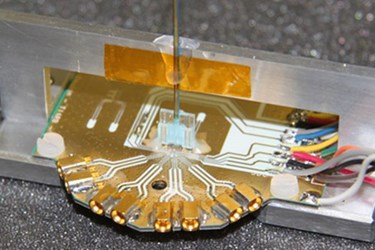
The 4x25Gbit/s hybrid integrated Rx, assembled by a project partner, CIP Technologies
The research leading to these results has received funding from the European Community’s Seventh Framework program C3PO [FP7/2010-2013] under grant agreement n°257377. C3PO (Colourless and Coolerless Components for low Power Optical Networks, www.greenc3po.eu) aims to design and develop a new generation of energy-efficient photonic and electronic components and apply them to next-generation access and high-speed metro-core networks. In the future, this work will be continued in ongoing European projects (FP7 MIRAGE, FP7 DISCUS, FP7 PhoxTrot and FP7 SPIRIT), with focus on the development of even faster ICs for electro-optic front-ends.
