Scanning Microwave Microscopy For Non-Destructive Imaging Of Silicon Nanostructures
By Jof Enriquez,
Follow me on Twitter @jofenriq

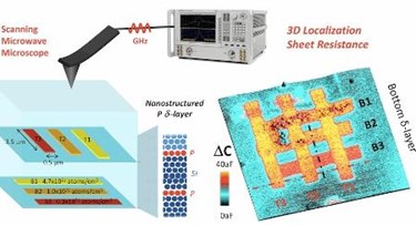
Academe and industry collaborators in Europe have developed a scanning microwave microscope capable of imaging three-dimensional, atom-sized components buried within silicon chips, making it one of the first devices to image and characterize, in a non-destructive way, those structures that are considered building blocks of quantum devices.
Advanced fabrication techniques have made it possible to create atomically thin regions of dopant atoms in silicon, which are key components of next-generation classical electrical devices, and of emerging quantum information systems, for their ability to produce quantum confinement in one, two, or three dimensions, and harnessed for device operation.
However, these tiny components are difficult to image and characterize using existing imaging technologies.
With scanning microwave microscopy (SMM), though, engineers can both image and characterize these components buried under the surface of the silicon chip. One microscope of this type developed recently focuses microwaves to a metal tip, which then is pushed against the surface of the chip. The microwaves fired into the chip bounce back to reveal a picture of the atomically thin phosphorus layers buried 5-15 nm below the silicon surface.
"The SMM measurements, which are completely nondestructive and sensitive to as few as 1900 to 4200 densely packed P atoms 4 to 15 nm below a silicon surface, yield electrical and geometric properties in agreement with those obtained from electrical transport and secondary ion mass spectroscopy for unpatterned phosphorus δ layers containing ~1013 P atoms. The imaging resolution was 37 ± 1 nm in lateral and 4 ± 1 nm in vertical directions, both values depending on SMM tip size and depth of dopant layers," the European researchers wrote in Science Advances.
One of the journal article's co-authors, Dr. Neil Curson, said, "The work is potentially of global significance because silicon chips are becoming so sophisticated and intricate that taking snapshots of their smallest working parts is incredibly difficult and time consuming, and currently involves destroying the chip. If we could easily see all components of a chip, in a non-destructive manor, it would be a game-changer."
"Another important application of our imaging technology is in assisting in the fabrication of phosphorus-in-silicon quantum computers, which have the potential to revolutionize computing completely, if realized," said Dr. Curson, who led the team at London Centre of Nanotechnology, University College London.
Johannes Kepler University, Keysight Technologies (Austria), Paul Scherrer Institut, ETH Zürich, and EPF Lausanne (Switzerland) collaborated with LCN on the project.
