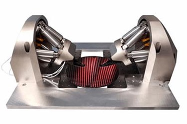
Fast Optical Alignment For SiP Production
Source: PI (Physik Instrumente) LP

Within converging photonics and semiconductor technologies, many of the practical challenges in testing and packaging have not been addressed. Testing and packaging of silicon photonics elements require nanoscale alignments that cannot be performed using visual or mechanical references. This blog article presents PI’s solution that addresses the need for fast, parallel, nanoscale-accurate, multi-DOF global optical alignment optimization required in key SiP production steps from planar testing to packaging.
access the Article!
Log In
Get unlimited access to:
Trend and Thought Leadership Articles

Case Studies & White Papers

Extensive Product Database

Members-Only Premium Content

Welcome Back! Please Log In to Continue.
X
Enter your credentials below to log in. Not yet a member of Photonics Online? Subscribe today.
Subscribe to Photonics Online
X
Subscribe to Photonics Online
PI (Physik Instrumente) LP
This website uses cookies to ensure you get the best experience on our website. Learn more
